


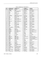


Interfaces and Connectors
EBX-41 Reference Manual
44
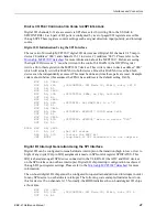
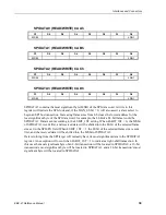
'D2 LSBIT_1ST = 0 SPI Shift Direction (Left Shifted)
'D1 0 = 0 This bit has no function
'D0 0 = 0 This bit has no function
OUT SPICONTROL2, &H30
'INITIALIZE MCP23S17
'===================
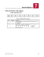
'MCP23S17 IOCON Register
'-----------------------
'D7 BANK = 0 Registers in same bank (addresses are sequential)
'D6 MIRROR = 1 The INT pins are internally connected
'D5 SEQOP = 0 Sequential op disabled. Addr ptr does not increment.
'D4 DISSLW = 0 Slew rate control for SDA output (enabled)
'D3 HAEN = 0 Hardware address enable (addr pins disabled)
'D2 ODR = 1 INT pin is open-drain
'D1 INTPOL = 0 Polarity of INT output pin (ignored when ODR=1)
'D0 0 = 0 This bit has no function
OUT SPIDATA1, &H44
'MCP23S17 IOCON Register Address
'-------------------------------
OUT SPIDATA2, &HA
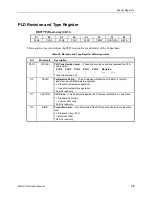
'MCP23S17 SPI Control Byte (Write)
'---------------------------------
'D7 SLAVEFA3 = 0 Slave Address (Fixed Portion)
'D6 SLAVEFA2 = 1 " " " "
'D5 SLAVEFA1 = 0 " " " "
'D4 SLAVEFA0 = 0 " " " "
'D3 SLAVEHA2 = 0 Slave Address Bits (Hardware Address Bits)
'D2 SLAVEHA1 = 0 " " " "
'D1 SLAVEHA0 = 0 " " " "
'D0 READWRITE = 0 Read/Write Bit = Write
OUT SPIDATA3, &H40
WHILE (INP(SPISTATUS) AND &H1) = &H1: WEND
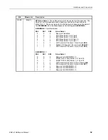
'INITIALIZE DIRECTION OF DIO LINES D15-D8 AS INPUTS
'==================================================
'Direction = All Inputs
OUT SPIDATA1, &HFF
'MCP23S17 IODIRA Register Address
OUT SPIDATA2, &H0
'MCP23S17 SPI Control Byte (Write)
OUT SPIDATA3, &H40
WHILE (INP(SPISTATUS) AND &H1) = &H1: WEND
'Repeat until ESC key is pressed
WHILE INKEY$ <> CHR$(27)
'READ DIO INPUT DATA FROM MCP23S17
'---------------------------------
'MCP23S17 GPIOA Register Address
OUT SPIDATA2, &H12
'MCP23S17 SPI Control Byte (Read)
OUT SPIDATA3, &H41


