

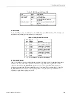


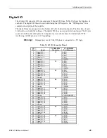


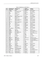


Interfaces and Connectors
EBX-41 Reference Manual
37
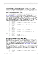
A
NALOG
I
NPUT
U
SING THE
SPI
I
NTERFACE
See "SPI Registers" for a description of the SPI interface and registers.
Initiating an Analog Conversion Using the SPI Interface
The following procedure can be used to initiate an analog conversion using the SPI interface
1.
Set ADIOMODE = 1 for the A/D converter for channels 9-16. The A/D converter for
channels 1-8 can be accessed for either setting of ADIOMODE.
2.
For the A/D converter for channels 1-8 write 15h to the SPICONTROL register (I/O
address CA8h) or write 13h for the A/D converter for channels 9-16. This value
configures the SPI port to select the on-board A/D converter, 16-bit frame length, low
SCLK idle state, rising edge SCLK edge, and automatic slave select.
3.
Write 10h to the SPISTATUS register (I/O address CA9h) – This value selects 2 MHz
SCLK speed, hardware IRQ disable, and left-shift data. A 2 MHz clock is used to avoid
having to insert a delay after the SPI cycle to wait for the end of the 4 µs A/D signal
acquisition interval. If a 4 MHz SPI clock is used then there must be a delay of 1.5 µs
after the SPI cycle ends before starting an A/D conversion; if an 8 MHz SPI clock is
used then there must be a delay of 2.75 µs after the end of the SPI cycle.
4.
Write any value to SPIDATA2 (I/O address CACh) – This data will be ignored by the
A/D converter.
5.
Write bit 0 of the analog input channel number to Bit 6, bits 2-1 of the analog input
channel number to bits 5-4, and a 2-bit input range code to bits 3-2 of SPIDATA3 (I/O
address CADh) – Any write operation to this register triggers an SPI transaction. The 2-
bit input-range codes are 0 (±5V), 1 (±10V), 2 (0 to +5V) or 3 (0 to +10V). Bit 7 must
be set to a ‘1’ for a single-ended channel (fyi - each A/D can be configured for either 8
single-ended inputs or 4 differential inputs). For example, if converting the 4th A/D
channel (channel number 3) with a 0 to +5V range then SPIDATA3 is set to D8h
6.
Poll the SPI BUSY bit in the SPISTATUS register until the conversion is completed.
7.
For the A/D converter for channels 1-8 write a ‘1’ to ADCONVST0 Bit 0 of the FPGA
ADC, DAC control/status register (I/O address CAFh) to start a conversion. For the A/D
converter for channels 9-16 write a ‘1’ to the ADCONVST1 bit 1.For the A/D converter
for channels 1-8 poll the ADCBUSY0 Bit 2 of the FPGA ADC/DAC control/status
register (I/O address CAFh) until this bit is a ‘0’ (not busy) to indicate a conversion is
completed (a conversion takes a maximum of 5 µs). For the A/D converter for channels
9-16 poll the ADCBUSY1 Bit 3.Read the conversion data from SPIDATA2 (upper 8 bits
of the 12-bit conversion) and SPIDATA3 (lower 4 bits of the 12-bit conversion are in the
upper 4 bits of this byte). The data read is from the previous conversion not the one for
the SPI values written in Steps 1–5. Another conversion cycle is required to retrieve that
data. Typically a number of channels are sampled at one time so this conversion delay is
not significant.
Anytime an SPI command is written to the A/D device a conversion must be issued for that
command. Another command will not be accepted until a conversion is performed.


