background image

SARA-G3 and SARA-U2 series - System Integration Manual 

UBX-13000995 - R08 

Objective Specification 

System description 


Page 23 of 188


Time [ms]

RX   

slot

unused 

slot

TX           

slot

TX   

slot

TX                  

slot

TX            

slot

MON       

slot

unused 

slot

RX  

slot

unused 

slot

TX         

slot

TX   

slot

TX                                   

slot

TX              

slot

MON   

slot

unused 

slot

GSM frame             

4.615 ms                                       

(1 frame = 8 slots)

Current [A]

60-120mA

GSM frame             

4.615 ms                                       

(1 frame = 8 slots)

1.5

1.0

0.5

0.0

60-120mA

10-40mA

200mA

Peak current 

depends on 

TX power

1600 mA


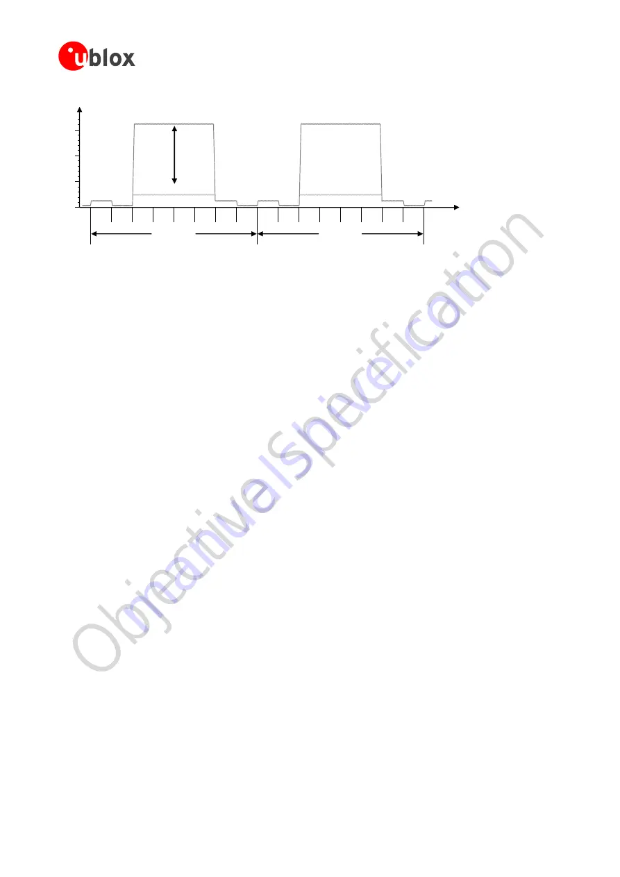
Figure 9: VCC current consumption profile versus time during a GPRS multi-slot class 12 connection (4 TX slots, 1 RX slot) 

 
For detailed current consumption values during 2G single-slot or multi-slot connection see 

SARA-G3 series Data 

Sheet

 [1] and 

SARA-U2 series Data Sheet

 [2]. 

Summary of Contents for SARA-G3

Page 1: ...ular modules and the SARA U2 GSM EGPRS HSPA cellular modules These modules are complete and cost efficient solutions offering voice and or data communication over diverse cellular radio access technol...

Page 2: ...13002 SARA G350 ATEX SARA G350 00X 00 08 49 GSM G2 TN 13002 SARA U260 SARA U260 00S 00 TBD TBD SARA U270 SARA U270 00S 00 TBD TBD SARA U280 SARA U280 00S 00 TBD TBD SARA U290 SARA U290 00S 00 TBD TBD...

Page 3: ...ation Manual provides the necessary information to successfully design in and configure these u blox cellular modules This manual has a modular structure It is not necessary to read it from the beginn...

Page 4: ...nal input EXT32K 37 1 6 5 Internal 32 kHz signal output 32K_OUT 37 1 7 Antenna interface 38 1 7 1 Antenna RF interface ANT 38 1 7 2 Antenna detection interface ANT_DET 39 1 8 SIM interface 39 1 8 1 U...

Page 5: ...2 2 2 2 RTC supply V_BCKP 93 2 2 3 Interface supply V_INT 95 2 3 System functions interfaces 96 2 3 1 Module power on PWR_ON 96 2 3 2 Module reset RESET_N 97 2 3 3 32 kHz signal EXT32K and 32K_OUT 98...

Page 6: ...6 3 Antenna checklist 153 3 Handling and soldering 154 3 1 Packaging shipping storage and moisture preconditioning 154 3 2 Handling 154 3 3 Soldering 155 3 3 1 Soldering paste 155 3 3 2 Reflow solderi...

Page 7: ...ion 170 A 4 Hardware migration 170 A 4 1 Supply interfaces 170 A 4 2 System functions interfaces 171 A 4 3 Antenna interface 172 A 4 4 SIM interface 173 A 4 5 Serial interfaces 173 A 4 6 Audio interfa...

Page 8: ...rich feature set including an extensive set of internet protocols dual stack IPv4 IPv6 and access to u blox GNSS positioning chips and modules with embedded A GPS AssistNow Online and AssistNow Offlin...

Page 9: ...3 reports a summary of 3G cellular characteristics of SARA U2 series modules Item SARA U260 SARA U270 SARA U280 SARA U290 Protocol stack 3GPP Release 7 3GPP Release 7 3GPP Release 7 3GPP Release 7 UE...

Page 10: ...sections and the available interfaces Memory V_BCKP RTC V_INT I O 32 kHz 26 MHz RF Transceiver Power Management ANT SAW Filter Switch VCC Supply 32 kHz Auxiliary UART SIM UART Power On Reset Cellular...

Page 11: ...Memory V_BCKP RTC V_INT I O RF Transceiver Power Management Cellular BaseBand Processor ANT VCC Supply USB DDC I2C SIM card detection SIM UART Power On Reset Digital audio I2S GPIO Antenna detection...

Page 12: ...section is composed of the following main elements Baseband processor a mixed signal ASIC which integrates Microprocessor for controller functions DSP core for 2G 3G Layer 1 and audio processing Dedic...

Page 13: ...onal description See section 2 2 3 for external circuit design in System PWR_ON All 15 I Power on input High input impedance input voltage level has to be properly fixed e g adding external pull up Se...

Page 14: ...1 9 1 for functional description See section 2 6 1 for external circuit design in TXD All 12 I UART data input 1 8 V input Circuit 103 TXD in ITU T V 24 for AT data FOAT on SARA G3 series modules for...

Page 15: ...differential impedance Pull up pull down and series resistors as required by USB 2 0 specifications 14 are part of the USB pin driver and need not be provided externally See section 1 9 3 for function...

Page 16: ...dset and loudspeaker mode See section 1 10 1 for functional description See section 2 7 1 for external circuit design in SPK_N SARA G340 SARA G350 45 O Differential analog audio output negative Differ...

Page 17: ...tion 1 11 for functional description See section 2 8 for external circuit design in GPIO4 SARA G340 SARA G350 SARA U2 25 I O GPIO 1 8 V GPIO by default configured to provide the custom GNSS RTC sharin...

Page 18: ...ower off mode from active mode When in power off mode the modules can be switched on by PWR_ON RESET_N or RTC alarm see 2 3 1 the module switches from power off to active mode When VCC supply is remov...

Page 19: ...rom active mode to connected mode Connected A voice call or a data call is in progress The module is ready to communicate with an external device by means of the application interfaces unless power sa...

Page 20: ...below the normal operating range minimum limit Ensure that the input voltage at VCC pins is above the minimum limit of the normal operating range for at least more than 3 s after the module switch on...

Page 21: ...for 576 9 s width of the transmit slot burst with a periodicity of 4 615 ms width of 1 frame 8 slots burst so with a 1 8 duty cycle according to GSM TDMA Time Division Multiple Access If the module is...

Page 22: ...evel the consumption can reach a quite high peak but lower than the one achievable in 2G single slot mode This happens for 1 154 ms width of the 2 Tx slots bursts in case of multi slot class 10 or for...

Page 23: ...MON slot unused slot GSM frame 4 615 ms 1 frame 8 slots Current A 60 120mA GSM frame 4 615 ms 1 frame 8 slots 1 5 1 0 0 5 0 0 60 120mA 10 40mA 200mA Peak current depends on TX power 1600 mA Figure 9...

Page 24: ...fers from the TDMA implemented in the 2G case In the worst scenario corresponding to a continuous transmission and reception at maximum RF output power approximately 250 mW or 24 dBm the average curre...

Page 25: ...rom 32 kHz to the 26 MHz used in active mode The time period between two paging block receptions is defined by the network This is the paging period parameter fixed by the base station through broadca...

Page 26: ...3 4 mA Active Mode Enabled Idle Mode Enabled 3 4 mA 60 120 mA 0 44 2 09 s IDLE MODE 20 30 ms ACTIVE MODE Time s Current mA 100 50 0 Time ms Current mA 100 50 0 4 5 mA 60 120 mA RX Enabled 20 40 mA DSP...

Page 27: ...ut pin is fed by external 32 kHz signal with characteristics compliant to the one specified in SARA G3 series Data Sheet 1 or by the 32K_OUT output pin provided by these modules when power saving is d...

Page 28: ...eception ACTIVE MODE 10 18 mA 60 120 mA 2G case 0 47 2 12 s 3G case 0 64 5 12 s Paging period Time s Current mA 100 50 0 Time ms Current mA 100 50 0 10 18 mA 60 120 mA RX Enabled 20 40 mA DSP Enabled...

Page 29: ...eries Data Sheet 2 and for SARA G300 SARA G310 modules only when their EXT32K input pin is fed by an external 32 768 kHz signal with proper characteristics specified in the EXT32K pin characteristics...

Page 30: ...5 3 Generic digital interfaces supply output V_INT The same 1 8 V voltage domain used internally to supply the generic digital interfaces of SARA G3 and SARA U2 series modules is also available on the...

Page 31: ...hen the VCC voltage stabilizes at its nominal value within the normal range The status of the PWR_ON input pin of SARA G3 and SARA U2 series modules while applying the VCC module supply is not relevan...

Page 32: ...all the digital pins of the modules are held in reset state When the internal reset signal is released by the integrated power management unit the processor core starts to configure the digital pins o...

Page 33: ...e When the internal reset signal is released by the integrated power management unit the processor core starts to configure the digital pins of the modules to each default operational state The durati...

Page 34: ...he appplication as by the AT CPWROFF command waiting the command response for a proper time period see u blox AT Commands Manual 3 and then a proper VCC supply must be held at least until the end of t...

Page 35: ...except the RTC supply V_BCKP Then the module remains in power off mode as long as a switch on event does not occur e g applying a proper low level to the PWR_ON input or applying a proper low level t...

Page 36: ...low from the external The pull up is internally biased by V_INT on SARA G3 modules and is biased by V_BCKP on SARA U2 modules A series Schottky diode is mounted inside the SARA G3 modules increasing t...

Page 37: ...s not powered or switched off if the EXT32K input is fed by a proper external 32 kHz signal SARA G3 series Data Sheet 1 describes the detailed electrical characteristics of the EXT32K input pin The 32...

Page 38: ...equency Range See the SARA G3 series Data Sheet 1 and the SARA U2 series Data Sheet 2 The required frequency range of the antenna depends on the operating bands of the used modules V S W R Return Loss...

Page 39: ...hip Both 1 8 V and 3 V SIM types are supported activation and deactivation with automatic voltage switch from 1 8 V to 3 V is implemented according to ISO IEC 7816 3 specifications The VSIM supply out...

Page 40: ...compatible signal levels 0 V for low data bit or ON state and 1 8 V for high data bit or OFF state For detailed electrical characteristics see SARA G3 series Data Sheet 1 and SARA U2 series Data Sheet...

Page 41: ...odules support the one shot automatic frame recognition in conjunction with one shot autobauding SARA G3 series modules automatic frame recognition and SARA U2 series modules one shot automatic frame...

Page 42: ...ICF 0 Automatic frame format recognition enabled by default on SARA G3 series One shot automatic frame format recognition enabled by default on SARA U2 series AT K3 HW flow control enabled by default...

Page 43: ...eceived The module drives the CTS line to the ON state or to the OFF state when it is either able or not able to accept data from the DTE over the UART see 1 9 1 4 for more details If hardware flow co...

Page 44: ...power idle mode whenever possible For more details see section 1 9 1 4 and u blox AT Commands Manual 3 AT UPSV command DSR signal behavior If AT S1 is set as it is by default the DSR module output li...

Page 45: ...When the remote DCE accepts the data call the module DCD line is set to ON and the CONNECT communication baudrate string is returned by the module At this stage the DTE can send characters through the...

Page 46: ...n each event independently triggers the RI line although the line will not be deactivated between each event As a result the RI line may stay to ON for more than 1 s If an incoming call is answered wi...

Page 47: ...by the module is correctly received by the DTE 0 Enabled AT K3 OFF ON or OFF Data sent by the DTE is correctly received by the module Data sent by the module is buffered by the module and will be corr...

Page 48: ...command is issued by the DTE the UART is disabled after the timeout set by the second parameter of the UPSV AT command for more details see u blox AT commands Manual 3 On SARA U2 modules when the AT U...

Page 49: ...r 20 ms and then if data has not been received or sent the UART is disabled for 2 1 s on SARA G3 modules or for 2 5 s on SARA U2 modules and afterwards the interface is enabled again The module active...

Page 50: ...RT is kept enabled On SARA G3 modules the CTS output line indicates the power saving state as illustrated in Figure 25 even with AT UPSV 2 AT UPSV 3 power saving enabled and controlled by the DTR line...

Page 51: ...is set with HW flow control disabled and the RTS line is set OFF On SARA U2 series the TXD input line is configured to wake up the system via data reception only if o AT UPSV 1 is set with hardware fl...

Page 52: ...ne the first character is not ignored if the module is in active mode i e the module replies OK or it represents the wake up character if the module is in low power idle mode i e the module does not r...

Page 53: ...SIM Access Profile not available on SARA G3 series modules For more details refer to Mux implementation Application Note 23 1 9 2 Auxiliary asynchronous serial interface UART AUX The auxiliary UART i...

Page 54: ...e u blox EasyFlash tool or by means of AT command for more details see section 1 13 13 and Firmware update application note 25 Audio over USB capabilities can be enabled by specific AT command refer t...

Page 55: ...interfaces The modules are capable of USB remote wake up signaling i e it may request the host to exit suspend mode or selective suspend by using electrical signaling to indicate remote wake up This...

Page 56: ...the module automatically enters idle mode whenever possible With the GNSS data ready function the GNSS receiver can indicate to the cellular module that it is ready to send data by the DDC I 2 C inter...

Page 57: ...the downlink audio signal can be changed with dedicated AT commands for each uplink or downlink path and then stored in two profiles in the non volatile memory refer to u blox AT Commands Manual 3 for...

Page 58: ...irectly drive a 8 or 4 loudspeaker for the hands free mode SARA G3 series Data Sheet 1 provides the detailed electrical characteristics of the analog audio downlink path Warning excessive sound pressu...

Page 59: ...t support the I2S_sample_rate parameter of AT UI2S the sample rate is fixed at 8 kHz only The main_uplink and main_downlink parameters of the AT USPM command must be properly configured to select the...

Page 60: ...edge I 2 S receive data changes on I 2 S clock falling edge 1 10 2 2 I 2 S interface Normal I 2 S mode Normal I 2 S supports 16 bits word Mono interface Sample rate I2S_sample_rate parameter Main fea...

Page 61: ...lar Buffer Sidetone Digital Gain DAC ADC Tone Generator AMR Player Hands Free Voiceband Sample Buffer Figure 28 SARA G340 SARA G350 modules audio processing system block diagram The sample based voice...

Page 62: ...e inside the baseband chipset The external digital audio devices can be interfaced directly to the DSP digital processing part via the I 2 S digital interface With exception of the speech encoder deco...

Page 63: ...o Discontinuous transmission DTX GSM 46 031 46 041 46 081 and 46 093 standards o Voice activity detection VAD GSM 46 032 46 042 46 082 and 46 094 standards o Background noise calculation GSM 46 012 46...

Page 64: ...ation function The Network status indication mode can be provided only on one pin per time it is not possible to simultaneously set the same mode on another pin The pin configured to provide the Netwo...

Page 65: ...u blox GNSS receiver connected to the cellular module setting the parameter gpio_mode of AT UGPIOC command to 5 The pin configured to provide the GNSS RTC sharing function is set as o Output to provid...

Page 66: ...command for further details see u blox AT Commands Manual 3 SARA G3 series do not support Module operating mode indication I2 S digital audio interface The I2S_RXD I2S_TXD I2S_CLK I2S_WA pins of SARA...

Page 67: ...PIO By default the pin is configured as Pin disabled Can be alternatively configured by the AT UGPIOC command as Output Input Network Status Indication GNSS Supply Enable GSM Tx Burst Indication Modul...

Page 68: ...nt function Can be alternatively configured by the UGPIOC command as Output Input Pin disabled 35 SARA U2 series I2S_TXD GPIO By default the pin is configured to provide I2 S data output function Can...

Page 69: ...es can experience various kind of out of coverage conditions limited service conditions when roaming to networks not supporting the specific SIM limited service in cells which are not suitable or barr...

Page 70: ...e system of the module SARA U2 series modules support also Secure File Transfer Protocol functionalities providing SSL encryption For more details about AT commands see the u blox AT Commands Manual 3...

Page 71: ...thout the root certificate verification o do not support the mutual authentication use of client certificates Table 14 lists the TLS cipher suite registry values supported by SARA U2 series modules SS...

Page 72: ...olds to identify the actual working temperature range Temperature measurement is done inside the module the measured value could be different from the environmental temperature Ta Warning area t 1 t 1...

Page 73: ...IF emerg call in progress Shut the device down Yes No Yes Yes No No No Yes Send shutdown notification Feature enabled full logic or indication only IF Full Logic Enabled Feature disabled no action Tem...

Page 74: ...lete assembly t 2 High temperature shutdown 95 C Equal to the internal temperature Ti measured in the worst case operating condition at typical supply voltage when the ambient temperature Ta in the re...

Page 75: ...he device position estimation based on the parameters of the mobile network cells visible to the specific device To estimate its position the module sends the CellLocate TM server the parameters of ne...

Page 76: ...GNSS receiver or the position estimated from CellLocate The choice depends on which positioning method provides the best and fastest solution according to the user configuration exploiting the benefi...

Page 77: ...ia a security signature during the download The firmware is then installed overwriting the current version In case of power loss during this phase the boot loader detects a fault at the next wake up a...

Page 78: ...rding the In Band modem solution for the European eCall and the Russian ERA GLONASS emergency call applications see the u blox eCall ERA GLONASS Application Note 29 1 13 16 SIM Access Profile SAP Not...

Page 79: ...uetooth Interface Bluetooth Transceiver Device including SIM Remote SIM Mobile Equipment SAP Server Bluetooth Transceiver Figure 34 Remote SIM access via Bluetooth and wired connection The application...

Page 80: ...ck which is generated by The internal 32 kHz oscillator in case of SARA G340 SARA G350 and SARA U2 modules The 32 kHz signal provided at the EXT32K input pin in case of SARA G300 and SARA G310 modules...

Page 81: ...DET pins Accurate design is required to guarantee SIM card functionality and compliance with applicable conformance standards reducing also the risk of RF coupling Carefully follow the suggestions pro...

Page 82: ...primary supply source has a nominal voltage much higher e g greater than 5 V than the modules VCC operating supply voltage The use of switching step down provides the best power efficiency for the ov...

Page 83: ...or battery the required capacitance can be considerably larger than 1 mF and the required ESR can be in the range of few tens of m Carefully evaluate the implementation of this solution since aging a...

Page 84: ...lied by a step down switching regulator capable of delivering to VCC pins the specified maximum peak pulse current with low output ripple and with fixed switching frequency in PWM mode operation great...

Page 85: ...063 W RC0402FR 07910RL Yageo R3 82 Resistor 0402 5 0 063 W RC0402JR 0782RL Yageo R4 8 2 k Resistor 0402 5 0 063 W RC0402JR 078K2L Yageo R5 39 k Resistor 0402 5 0 063 W RC0402JR 0739KL Yageo U1 Step D...

Page 86: ...voltage supply application circuit using an LDO linear regulator Reference Description Part Number Manufacturer C1 C2 10 F Capacitor Ceramic X5R 0603 20 6 3 V GRM188R60J106ME47 Murata R1 47 k Resisto...

Page 87: ...end of a transmit burst during a single slot 2G voice data call when current consumption on the VCC supply can rise up to the maximum peak pulse current specified in the SARA G3 series Data Sheet 1 o...

Page 88: ...s modules do not have an on board charging circuit In the application circuit example described in Figure 40 a rechargeable Li Ion or Li Polymer battery pack that features proper pulse and DC discharg...

Page 89: ...MLE 18G Bourns R1 R2 24 k Resistor 0402 5 0 1 W RC0402JR 0724KL Yageo Phycomp R3 3 3 k Resistor 0402 5 0 1 W RC0402JR 073K3L Yageo Phycomp R4 1 0 k Resistor 0402 5 0 1 W RC0402JR 071K0L Yageo Phycomp...

Page 90: ...s supply source for the module and starts a charging phase accordingly The MP2617 IC normally provides a supply voltage to the module regulated from the external main primary source allowing immediate...

Page 91: ...Li Polymer battery charging and power path management application circuit Reference Description Part Number Manufacturer B1 Li Ion or Li Polymer battery pack with 10 k NTC Various manufacturer C1 C5...

Page 92: ...connected to RF Power Amplifiers voltage ripple at high frequency may result in unwanted spurious modulation of transmitter RF signal This is more likely to happen with switching DC DC converters in w...

Page 93: ...A G3 series SARA U2 series B3 c 2 V_BCKP Figure 43 Real time clock supply V_BCKP application circuits a using a 100 F capacitor to let the RTC run for 1 minute after VCC removal b using a 70 mF capaci...

Page 94: ...RA G310 modules the V_BCKP supply output can be used to supply an external 32 kHz oscillator which provides a 32 kHz signal to the EXT32K input pin as reference clock for the RTC timing so that the mo...

Page 95: ...G3 series or 70 mVpp SARA U2 series in low power idle mode when the switching regulator operates in PFM mode It is not recommended to supply sensitive analog circuitry without adequate filtering for...

Page 96: ...n open drain output on the external device with an external pull up resistor e g 100 k biased by the V_BCKP supply pin of the module as described in Figure 44 and Table 23 A compatible push pull outpu...

Page 97: ...ding to JESD22 A114 Higher protection level can be required if the line is externally accessible on the application board e g if an accessible push button is directly connected to RESET_N pin Higher p...

Page 98: ...o the section 1 5 1 4 and to the SARA G3 series Data Sheet 1 and can provide the RTC functions when the module is switched on 24 32K_OUT SARA G300 SARA G310 31 EXT32K Figure 46 EXT32K application circ...

Page 99: ...not available on SARA G340 and SARA G350 modules since the internal oscillator generates the 32 kHz RTC reference clock ESD sensitivity rating of the EXT32K input pin and the 32K_OUT output pin is 1...

Page 100: ...able 50 connector providing proper PCB to RF cable transition it is recommended to strictly follow the layout and cable termination guidelines provided by the connector manufacturer Integrated antenna...

Page 101: ...ld be free of digital lines Increase GND keep out i e clearance a void area around the ANT pad on the top layer of the application PCB to at least 250 m up to adjacent pads metal definition and up to...

Page 102: ...finite element method solver for electromagnetic structures from Ansys Corporation or using freeware tools like AppCAD from Agilent www agilent com or TXLine from Applied Wave Research www mwoffice c...

Page 103: ...nal routing in parallel to transmission line or crossing the transmission line on buried metal layer Do not route microstrip line below discrete component or other mechanics placed on top layer Two ex...

Page 104: ...ntenna manufacturer providing the best possible return loss or V S W R Provide a ground plane large enough according to the related integrated antenna requirements the ground plane of the application...

Page 105: ...K73H1ETTP1002F KOA Speer J1 SMA Connector 50 Through Hole Jack SMA6251A1 3GT50G 50 Amphenol C3 SARA U2 15 pF Capacitor Ceramic C0G 0402 5 50 V GRM1555C1H150J Murata SARA G3 0 jumper 0402 Various Manuf...

Page 106: ...ty and avoid a reduction of module RF performance The choke inductor should exhibit a parallel Self Resonance Frequency SRF in the range of 1 GHz to improve the RF isolation of load resistor For examp...

Page 107: ...onnector by means of a 50 transmission line implementing the design guidelines described in section 2 4 1 and the recommendations of the SMA connector manufacturer DC blocking capacitor at the ANT pin...

Page 108: ...re suitable for applications where the SIM changing is required during the product lifetime A SIM card holder can have 6 or 8 positions if a mechanical card presence detector is not provided or it can...

Page 109: ...nce i e less than 10 pF ESD protection e g Tyco Electronics PESD0402 140 on each externally accessible SIM line close to each related pad of the SIM connector ESD sensitivity rating of the SIM interfa...

Page 110: ...rovide a bypass capacitor of about 22 pF to 47 pF e g Murata GRM1555C1H470J on each SIM line VSIM SIM_CLK SIM_IO SIM_RST to prevent RF coupling especially in case the RF antenna is placed closer than...

Page 111: ...ry close to each related pad of the SIM connector to prevent RF coupling especially in case the RF antenna is placed closer than 10 30 cm from the SIM card holder Provide a low capacitance i e less th...

Page 112: ...roviding proper connection between SIM switch and SIM chip as described in Figure 55 If it is required to switch between more than two SIM a circuit similar to the one described in Figure 57 can be im...

Page 113: ...citance and Low On Resistance FSA2567 Fairchild Semiconductor Table 30 Example of components for the connection to two removable SIM cards with SIM detection implemented 2 5 1 2 Guidelines for SIM lay...

Page 114: ...A U2 1 8V DCE 12 TXD 9 DTR 13 RXD 10 RTS 11 CTS 6 DSR 7 RI 8 DCD GND 0 TP 0 TP 0 TP 0 TP Figure 58 UART interface application circuit with complete V 24 link in DTE DCE serial communication 1 8 V DTE...

Page 115: ...interface application circuit with partial V 24 link 6 wire in the DTE DCE serial communication 1 8 V DTE If a 3 0 V application processor is used appropriate unidirectional voltage translators must b...

Page 116: ...terface is enabled by the RTS line as described in section 1 9 1 4 reaching very low current consumption With this configuration when the module is in idle mode the UART is re enabled 20 ms after RTS...

Page 117: ...tion when the module is in idle mode data transmitted by the DTE will be buffered by the DTE and will be correctly received by the module when active mode is entered If the HW flow control is disabled...

Page 118: ...t Number Manufacturer C1 C2 100 nF Capacitor Ceramic X7R 0402 10 16 V GRM155R61A104KA01 Murata U1 Unidirectional Voltage Translator SN74AVC2T245 Texas Instruments Table 34 Component for UART applicati...

Page 119: ...e g Texas Instruments SN74CB3Q16244 TS5A3159 or TS5A63157 between the two circuit connections and set to high impedance during module power down mode and during the module power on sequence ESD sensit...

Page 120: ...See Firmware Update Application Note 25 for additional guidelines regarding the procedure for SARA G3 modules firmware upgrade over the auxiliary UART interface using the u blox EasyFlash tool Any ext...

Page 121: ...cessible point on the line connected to this pin as described in Figure 68 and Table 36 The USB interface pins ESD sensitivity rating is 1 kV Human Body Model according to JESD22 A114F Higher protecti...

Page 122: ...mpedance ZCM is as close as possible to 30 Consider design rules for USB_D USB_D similar to RF transmission lines being them coupled differential micro strip or buried stripline avoid any stubs abrupt...

Page 123: ...nal DDC I 2 C pull ups to the V_INT 1 8 V supply source or another supply source enabled after V_INT e g as the GNSS 1 8 V supply present in Figure 71 application circuit as any external signal connec...

Page 124: ...s the u blox GNSS receiver to recover from a power breakdown with either a hot start or a warm start depending on the actual duration of the GNSS VCC outage and to maintain the configuration settings...

Page 125: ...out TCXO Additional filtering may be needed to properly supply an external LNA depending on the characteristics of the used LNA adding a series ferrite bead and a bypass capacitor e g the Murata BLM15...

Page 126: ...d using a proper Unidirectional General Purpose Voltage Translator e g TI SN74AVC2T245 which additionally provides the partial power down feature so that the 3 0 V GNSS supply can be also ramped up be...

Page 127: ...s the partial power down feature so that the 3 0 V GNSS supply can be also ramped up before the V_INT 1 8 V cellular supply The V_BCKP supply output of the cellular module can be directly connected to...

Page 128: ...n Application Note 24 and to the Hardware Integration Manual of the u blox GNSS receivers 2 6 4 2 Guidelines for DDC I 2 C layout design The DDC I 2 C serial interface requires the same consideration...

Page 129: ...io of the two resistance in one leg R2 R3 should be equal to the ratio of the two resistance in the other leg R4 MIC i e R2 has to be equal to R4 e g 2 2 k and R3 has to be equal to the microphone nom...

Page 130: ...Speaker Connector J2 Microphone Connector MIC J1 D4 D2 Figure 75 Analog audio interface headset and handset mode application circuit Reference Description Part Number Manufacturer C1 10 F Capacitor C...

Page 131: ...e stable operation of the internal regulator Connect the reference of the microphone circuit to the MIC_GND pin of the module as a sense line Provide a proper series capacitor at both MIC_P and MIC_N...

Page 132: ...5 V GRM1555C1H270JA01 Murata C8 C9 47 nF Capacitor Ceramic X7R 0402 10 16V GRM155R71C473KA01 Murata D1 D2 D3 D4 Low Capacitance ESD Protection CG0402MLE 18G Bourns J1 Microphone Connector Various Manu...

Page 133: ...circuit has to be inserted from the single ended output of the external audio device to the MIC_P MIC_N balanced input of the module as described in the Figure 77 right side 10 F series capacitors ar...

Page 134: ...l pair embedded in ground to reduce differential noise pick up The balanced configuration will help reject the common mode noise Route microphone reference as a signal line since the MIC_GND pin is in...

Page 135: ...crophone input signal to the digital bit stream over the digital audio interface The module s I 2 S interface I 2 S master is connected to the related pins of the external audio codec I 2 S slave The...

Page 136: ...necting the I 2 S digital audio interface of the SARA G340 SARA G350 and SARA U2 modules to an external audio voice codec using the same parts listed in Table 44 The module s I 2 S interface I 2 S mas...

Page 137: ...er down mode and during the module power on sequence ESD sensitivity rating of I 2 S interface pins is 1 kV Human Body Model according to JESD22 A114 Higher protection level could be required if the l...

Page 138: ...8 Network Indicator R3 GNSS Supply Enable GNSS Data Ready GNSS RTC Sharing 16 GPIO1 DL1 T1 Figure 80 GPIO application circuit Reference Description Part Number Manufacturer R1 47 k Resistor 0402 5 0 1...

Page 139: ...e application circuit Pin 33 RSVD must be connected to GND SARA G3 SARA U2 33 RSVD RSVD Figure 81 Application circuit for the reserved pins RSVD 2 10Module placement Optimize placement for minimum len...

Page 140: ...ding to application production process requirements K M1 M1 M2 E G H J E ANT pin B Pin 1 K G H J A D D O O L N L I F F K M1 M1 M2 E G H J E ANT pin B Pin 1 K G H J A D D O O L N L I F F Stencil 150 m...

Page 141: ...e overall temperature distribution is influenced by the configuration of the active components during the specific mode of operation and their different thermal resistance toward the case interface Mo...

Page 142: ...sink on the backside of the application board with forced air ventilation can be seen from the module temperature increase which now can be summarized as following for SARA G3 modules 1 C during a GSM...

Page 143: ...vice classification as defined by ETSI EN 301 489 1 19 Applicability of the ESD immunity test to the relative device ports or the relative interconnecting cables to auxiliary equipments depends on dev...

Page 144: ...are recommended and should be implemented in any device that integrates a SARA G3 and SARA U2 series module according to the application board classification see ETSI EN 301 489 1 19 to satisfy the r...

Page 145: ...o assure SIM interface functionality when an electrostatic discharge is applied to the application board enclosure It is suggested to use as short as possible connection lines at SIM pins Maximum ESD...

Page 146: ...e range section of the SARA G3 series Data Sheet 1 Even if the SARA G350 ATEX modules are certified as components intended for use in potentially explosive atmospheres as described above the applicati...

Page 147: ...odules according to the specific potentially explosive gas atmosphere category subdivision where the apparatus is intended for use The following maximum input and equivalent parameters must be conside...

Page 148: ...A G350 ATEX modules intended for use in potentially explosive atmospheres Any specific applicable requirement for the VCC supply circuit design must be fulfilled according to all the exact applicable...

Page 149: ...6pF SARA G300 SARA G310 52 VCC 53 VCC 51 VCC 100 F 2 V_BCKP GND GND GND RTC back up 1 8V DTE 1 8V DTE 16 RSVD 18 RESET_N Application Processor Open Drain Output 15 PWR_ON 100k Open Drain Output TXD RX...

Page 150: ...28 RXD_AUX 0 0 TP TP u blox 1 8 V GNSS Receiver 4 7k OUT IN GND LDO Regulator SHDN SDA SCL 4 7k 3V8 1V8_GPS SDA2 SCL2 GPIO3 GPIO4 TxD1 EXTINT0 26 27 24 25 47k VCC GPIO2 23 1 8V Digital Audio Device I2...

Page 151: ...1V8_GPS SDA2 SCL2 GPIO3 GPIO4 TxD1 EXTINT0 26 27 24 25 47k VCC GPIO2 23 RSVD RSVD RSVD RSVD 46 47 48 49 15pF 33 RSVD 31 RSVD 47pF SIM Card Holder CCVCC C1 CCVPP C6 CCIO C7 CCCLK C3 CCRST C2 GND C5 47...

Page 152: ...V_INT pin RESET_N and or PWR_ON pins for module FW upgrade by the u blox EasyFlash tool and for diagnostic purpose Provide accessible testpoints directly connected to the following pins of the SARA U...

Page 153: ...urce for VCC Design USB_D USB_D connection as 90 differential pair with 30 common mode impedance Route analog audio signals away from noisy sources primarily RF interface VCC switching supplies The au...

Page 154: ...e a small working station or a large manufacturing area The main principle of an EPA is that there are no highly charging materials near ESD sensitive electronics all conductive materials are grounded...

Page 155: ...he IPC 7530 Guidelines for temperature profiling for mass soldering reflow and wave processes published 2001 Reflow profiles are to be selected according to the following recommendations Failure to ob...

Page 156: ...cess 3 3 3 Optical inspection After soldering the SARA G3 and SARA U2 series modules inspect the modules optically to verify that the module is properly aligned and centered 3 3 4 Cleaning Cleaning th...

Page 157: ...and it is important to prevent them from flowing into the module The RF shields do not provide 100 protection for the module from coating liquids with low viscosity therefore care is required in appl...

Page 158: ...ion schemes the application device that integrates the modules must be approved under all the certification schemes required by the specific application device to be deployed in the market The require...

Page 159: ...ormity United States only This device complies with Part 15 of the FCC rules Operation is subject to the following two conditions this device may not cause harmful interference this device must accept...

Page 160: ...terference including interference that may cause undesired operation of the device Radio Frequency RF Exposure Information The radiated output power of the u blox Cellular Module is below the Industry...

Page 161: ...gst nsf eng sf08792 html IMPORTANT les fabricants d applications portables contenant les modules SARA G310 SARA G350 SARA U260 SARA U280 doivent faire certifier leur produit final et d poser directem...

Page 162: ...Annex IV of Directive 1999 5 EC has been followed with the involvement of the following Notified Body number 1588 Thus the following marking is included in the product There is no restriction for the...

Page 163: ...G350 ATEX modules are certified with the following marking Ex II 1G Ex ia IIC IIB The temperature range for using SARA G350 ATEX modules is defined in the Operating temperature range section of the SA...

Page 164: ...tests GPIOs digital interfaces Measurement and calibration of RF characteristics in all supported bands Receiver S N verification frequency tuning of reference clock calibration of transmitter and rec...

Page 165: ...ands Manual 3 AT CSQ command rssi ber parameters These kinds of test may be useful as a go no go test but not for RF performance measurements This test is suitable to check the communication with host...

Page 166: ...a interface and to check other device interfaces from which depends the RF performance To avoid module damage during transmitter test a proper antenna according to module specifications or a 50 termin...

Page 167: ...s for module damaging caused by an inappropriate use of this feature 2 Trigger TX GMSK burst at maximum PCL o To check if the power supply is correctly assembled and is able to deliver the required cu...

Page 168: ...RSVD MIC_N 28 29 30 31 32 33 34 35 36 37 38 76 75 74 73 72 71 70 69 68 67 66 LISA U1 series Top View GND RSVD GND GND GND GND GND ANT GND GND GND GND GND GND GND GND GND GND GND GND GND GND 65 64 63...

Page 169: ...the antenna detection function implementing an external application circuit between ANT_DET and ANT pins Check the module power on requirements Table 50 and relative section summarize differences betw...

Page 170: ...s in the current consumption figures The voltage provided must be within the normal operating range limits to allow module switch on and must be above the minimum limit of the extended operating range...

Page 171: ...odule 1 4 5 6 PWR_ON falling edge i e low pulse is required for LISA series but it is not required for SARA External pull up is not needed for LISA C2 series since internal pull up is provided Module...

Page 172: ...1750 1800 1850 1900 1950 2000 2050 2100 2150 2200 880 960 1710 1880 SARA G300 SARA G340 800 800 800 850 900 950 1900 1900 1700 1750 1800 1850 1900 1950 2000 2050 2100 2150 2200 824 894 1850 1990 LISA...

Page 173: ...les do not support DSR DCD and DTR functions Table 51 and the module s datasheet 1 4 5 6 report minor differences in the internal pull ups and drivers strengths These are the default settings of the U...

Page 174: ...I 2 C interface and clock reference by means of the CODEC_CLK pin For further details regarding analog audio interfaces characteristics usage and settings see the related module datasheet 1 4 5 6 Syst...

Page 175: ...G340 SARA G350 Input for antenna detection circuit Not Available Internal antenna detection circuit Internal antenna detection circuit System PWR_ON 15 No internal pull up L level 0 10 V 0 65 V H leve...

Page 176: ...trl output Driver strength 4 mA 1 8 V Flow ctrl output Driver strength 4 mA 1 8 V Flow ctrl output Driver strength 6 mA TXD 12 1 8 V Data input Internal pull up 102 A 15 1 8 V Data input Internal pull...

Page 177: ...only 1 8 V Data Out PCM Normal I2S mode Driver strength 2 5 mA 1 8 V Data Out PCM Normal I2S mode Driver strength 2 mA LISA U200 00S N A I2S_RXD 37 SARA G340 SARA G350 1 8 V Data In PCM Normal I2S mod...

Page 178: ...GPIO4 25 SARA G340 SARA G350 1 8 V configurable GPIO Default GNSS RTC shar Driver strength 6 mA Inner pull down 51 A 24 1 8 V configurable GPIO Default Pin disabled Driver strength 4 mA Inner pull do...

Page 179: ...series LISA U2 series GPIO13 Not Available 58 Not Available Not Available 1 8 V configurable GPIO Default SPI_SRDY Driver strength 6 mA Inner pull down 200 A GPIO14 Not Available 59 Not Available Not...

Page 180: ...GND SPK_P MIC_BIAS MIC_GND MIC_P GND VCC VCC RSVD I2S_TXD I2S_CLK SIM_CLK SIM_IO VSIM SIM_DET VCC MIC_N SPK_N SIM_RST I2S_RXD I2S_WA GND GND GND GND GND GND GND GND GND ANT_DET ANT SARA G340 SARA G35...

Page 181: ...ternal pull up 8 k No functional difference 13 RXD UART Data Output 1 8 V Driver strength 6 mA RXD UART Data Output 1 8 V Driver strength 6 mA No functional difference 14 GND Ground GND Ground 15 PWR_...

Page 182: ...ck Output SIM_CLK SIM Clock Output No functional difference 39 SIM_IO SIM Data I O SIM_IO SIM Data I O No functional difference 40 SIM_RST SIM Reset Output SIM_RST SIM Reset Output No functional diffe...

Page 183: ...8 SIM_CLK 40 SIM_RST 47pF SW1 SW2 4 V_INT 42 SIM_DET 470k ESD ESD ESD ESD ESD ESD 56 ANT 62 ANT_DET 10k 82nH 33pF Connector 27pF ESD External Antenna 1k TP u blox 1 8V GNSS Receiver 4 7k OUT IN GND LD...

Page 184: ...igital Signal Processing DSR Data Set Ready DTE Data Terminal Equipment DTM Dual Transfer Mode DTR Data Terminal Ready EMC Electro magnetic Compatibility EMI Electro magnetic Interference ESD Electro...

Page 185: ...MU Power Management Unit PSRAM Pseudo Static RAM PWM Pulse Width Modulation RF Radio Frequency RI Ring Indicator RTC Real Time Clock RTS Request To Send SAW Surface Acoustic Wave SIM Subscriber Identi...

Page 186: ...mentation Conformance Statement ICS 18 CENELEC EN 61000 4 2 2001 Electromagnetic compatibility EMC Part 4 2 Testing and measurement techniques Electrostatic discharge immunity test 19 ETSI EN 301 489...

Page 187: ...st revision with old doc number GSM G2 HW 12003 A 03 Jul 2013 sses Updated status to Advance Information Added integration description for SARA G350 ATEX modules Updated SARA G300 SARA G310 supported...

Page 188: ...te Ltd Phone 65 6734 3811 E mail info_ap u blox com Support support_ap u blox com Regional Office Australia Phone 61 2 8448 2016 E mail info_anz u blox com Support support_ap u blox com Regional Offic...

Reviews: