EVK-IRIS-W10 - User guide
UBX-23007837 - R03
Hardware description
Page 37 of 43
C1-Public
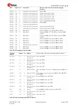
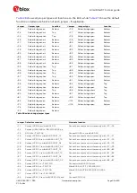
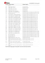
Header
GND
+3.3V
+5V
J3
10
2
1
J4
10
2
1
J44
10
J47
6,8,9,10
J48
10
J10
2
1
J70
2
1
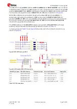
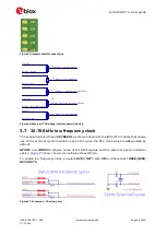
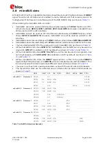
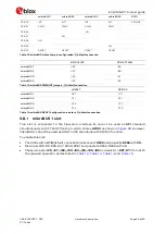
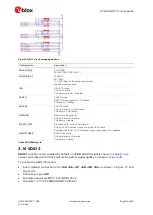
Table 24: Power signals mapping to the pin headers
3.12
QSPI memory
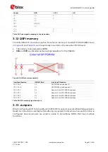
The EVK-IRIS-W10 provides an option for external memory. A Quad SPI PSRAM (
U2
), shown
can be optionally mounted on the rear side of EVK board.
•
The memory is as
powered by
+3
V
3.
•
C24
and
C47
are intended as decoupling capacitors for the PSRAM.
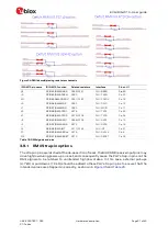
Figure 40: QSPI memory schematic
Interface function
IRIS-W10 pin
Interface IC function
QSPI-RCE
A5
QSPI SRAM slave select 0
QSPI-RCLK
A2
QSPI SRAM interface clock 0
QSPI-RD0
B4
Data bit 0 for QSPI SRAM interface
QSPI-RD1
A4
Data bit 1 for QSPI SRAM interface
QSPI-RD2
B3
Data bit 2 for QSPI SRAM interface
QSPI-RD3
A3
Data bit 3 for QSPI SRAM interface
Table 25: QSPI memory signals and pins
3.13
Jumpers
When configuring GPIO functionality, EVK-IRIS-W10 supports several solder-bridge jumpers.
Read the instructions carefully before altering any jumper to determine how each function is
configured. Several jumpers are wired in series to demultiplex GPIOs that have multiple
functions.

