background image

SARA-G3 series - System Integration Manual 

UBX-13000995 - R06 

Objective Specification 

Approvals 


Page 184 of 218


4.5


SARA-G350 ATEX conformance for use in explosive atmospheres 

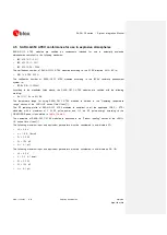
SARA-G350  ATEX  modules  are  certified  as  components  intended  for  use  in  potentially  explosive 
atmospheres compliant to the following standards: 


IEC 60079-0: 2011 


IEC 60079-11: 2011 


IEC 60079-26: 2006 

The certification number of SARA-G350 ATEX modules according to the ATEX directive 94/9/EC is: 


SIQ 13 ATEX 032 U  

The  certification  number  of  SARA-G350  ATEX  modules  according  to  the  IECEx  conformity  assessment 
system is: 


IECEx SIQ 13.0004U 

According to the standards listed above, the SARA-G350 ATEX modules are certified with the following 
marking: 


Ex II 1G, Ex ia IIC/IIB 

The  temperature  range  for  using  SARA-G350  ATEX  modules  is  defined  in  the  ‘Operating  temperature 
range’ section of the 

SARA-G3 series Data Sheet [1]. 

The RF radiating profile of SARA-G350 ATEX modules is compliant to all the applicable 3GPP / ETSI 
standards,  with  a  maximum  of  2  W  RF  pulse  power  and  1.15  mJ  RF  pulse  energy  according  to  the 
GSM/GPRS power class stated in 

Table 2Table 2

. 

The nameplate of SARA-G350 ATEX modules is described in the ‘Product labeling’ section of the 

SARA-

G3 series Data Sheet [1]. 
The following maximum input and equivalent parameters must be considered in sub-division IIC: 


Ui = 3.8 V 


Ii = 1.6 A (burst) 


Pi = 2.5 W 


Ci = 103 µF 


Li = 4.1 µH 

The following maximum input and equivalent parameters must be considered in sub-divisions IIB, IIA: 


Ui = 4.2 V 


Ii = 2.5 A (burst) 


Pi = 2.5 W 


Ci = 103 µF 


Li = 4.1 µH 


Summary of Contents for SARA-G3 Series

Page 1: ...he features and the system integration of SARA G3 series GSM GPRS wireless modules These modules are complete and cost efficient solutions offering up to quad band GSM GPRS voice and or data transmiss...

Page 2: ...nce Information This document contains data based on early testing Revised and supplementary data will be published later Early Production Information This document contains data from product verifica...

Page 3: ...tions at any time without notice u blox reserves all rights to this document and the information contained herein Reproduction use or disclosure to third parties without express permission is strictly...

Page 4: ...Integration Manual provides the necessary information to successfully design in and configure these u blox wireless modules This manual has a modular structure It is not necessary to read it from the...

Page 5: ...ful Information when Contacting Technical Support When contacting Technical Support have the following information ready Module type e g SARA G350 and firmware version Module configuration Clear descr...

Page 6: ...1 6 3 Module reset 3930 1 6 4 External 32 kHz signal input EXT32K 4031 1 6 5 Internal 32 kHz signal output 32K_OUT 4131 1 7 Antenna interface 4232 1 7 1 Antenna RF interface ANT 4232 1 7 2 Antenna det...

Page 7: ...8862 2 Design in 9063 2 1 Supply interfaces 9164 2 1 1 Module supply VCC 9164 2 1 2 RTC supply V_BCKP 10072 2 1 3 Interface supply V_INT 10374 2 2 System functions interfaces 10575 2 2 1 Module power...

Page 8: ...ic checklist 168123 2 15 2 Layout checklist 170124 2 15 3 Antenna checklist 170124 3 Handling and soldering 171125 3 1 Packaging shipping storage and moisture preconditioning 171125 3 2 Soldering 1711...

Page 9: ...ules 188139 A 1 Overview 188139 A 2 Checklist for migration 189140 A 3 Software migration 191141 A 4 Hardware migration 191141 A 4 1 Supply interfaces 191141 A 4 2 System functions interfaces 193142 A...

Page 10: ...00 are respectively quad band and dual band GSM GPRS wireless modules targeted for high volume cost sensitive applications providing GSM GPRS functionalities with a reduced set of additional features...

Page 11: ...ass B2 GSM GPRS Bands E GSM 900 MHz DCS 1800 MHz GSM 850 MHz E GSM 900 MHz DCS 1800 MHz PCS 1900 MHz GSM 850 MHz E GSM 900 MHz DCS 1800 MHz PCS 1900 MHz GSM GPRS Power Class Class 4 33 dBm for 900 Cla...

Page 12: ...ARA G310 SARA G350 Circuit Switched Data Rate Up to 9 6 kb s DL UL4 Transparent mode Non transparent mode Up to 9 6 kb s DL UL4 Transparent mode Non transparent mode Up to 9 6 kb s DL UL4 Transparent...

Page 13: ...Filter Switch PA VCC Supply 32 kHz Auxiliary UART SIM Card UART Power On Reset Figure 1 SARA G300 and SARA G310 modules block diagram Memory V_BCKP RTC V_INT I O 26 MHz 32 768 kHz RF Transceiver Powe...

Page 14: ...SARA G3 series System Integration Manual UBX 13000995 R06 Objective Specification System description Page 14 of 218...

Page 15: ...active mode or connected mode Baseband and Power Management section The Baseband and Power Management section is composed of the following main elements Baseband processor a mixed signal ASIC which i...

Page 16: ...ve Specification System description Page 16 of 218 G310 modules provides a 32 kHz reference signal suitable only to feed the EXT32K input pin furnishes the reference clock for the RTC and allows low p...

Page 17: ...put output V_BCKP 2 3 V typical generated by internal regulator when valid VCC supply is present See section 1 5 21 5 2 for functional description See section 2 1 22 1 2 for external circuit design in...

Page 18: ...for antenna detection ADC input for antenna detection function See section 1 7 2 for functional description See section 2 3 2 for external circuit design in SIM VSIM All 41 O SIM supply output VSIM 1...

Page 19: ...in ITU T V 24 for AT command data communication FOAT Internal active pull up to V_INT See section 1 9 11 9 1 for functional description See section 2 5 12 5 1 for external circuit design in DSR All 6...

Page 20: ...ITU T V 24 for FW upgrade and trace log capture Access by external test point is recommended Internal active pull up to V_INT See section 1 9 21 9 2 for functional description See section 2 5 22 5 2 f...

Page 21: ...acitor See section 1 10 11 10 1 for functional description See section 2 6 12 6 1 for external circuit design in MIC_P SARA G350 49 I Differential analog audio input positive Differential analog audio...

Page 22: ...disabled See section 1 111 11 for functional description See section 2 72 7 for external circuit design in GPIO2 SARA G350 23 I O GPIO 1 8 V GPIO by default configured to provide the custom GNSS supp...

Page 23: ...SARA G3 series System Integration Manual UBX 13000995 R06 Objective Specification System description Page 23 of 218...

Page 24: ...Internal RTC timer operates on SARA G350 modules only if a valid voltage is applied to V_BCKP pin Additionally a proper external 32 kHz signal must be fed to EXT32K pin on SARA G300 SARA G310 to let R...

Page 25: ...m occurs refer to u blox AT Commands Manual 2 AT CALA command Data received on UART interface refer to 1 9 1 4 RTS input line set to the ON state by the DTE if hardware flow control has been disabled...

Page 26: ...e is no activity for a defined time interval Any wake up event described in the module operating modes summary table above Incoming outgoing call or other dedicated device network communication Call t...

Page 27: ...ts listed in Table 6Table 6 The VCC supply circuit affects the RF compliance of the device integrating SARA G3 series module with applicable required certification schemes as well as antenna circuit d...

Page 28: ...al specific requirement for SARA G350 ATEX modules integration in potentially explosive atmospheres applications refer to section 2 13 1 5 1 2 VCC current consumption in connected mode When a GSM call...

Page 29: ...sed slot TX slot unused slot unused slot MON slot unused slot RX slot unused slot unused slot TX slot unused slot unused slot MON slot unused slot GSM frame 4 615 ms 1 frame 8 slots GSM frame 4 615 ms...

Page 30: ...ent consumption profiles in GPRS connected mode in the 850 or 900 MHz bands with 2 slots used to transmit and 1 slot used to receive Time ms RX slot unused slot unused slot TX slot TX slot unused slot...

Page 31: ...ordance to GSM system requirements When the module monitors the paging channel it wakes up to active mode to enable the reception of paging block In between the module switches to idle mode This is kn...

Page 32: ...00 SARA G310 modules with the EXT32K input fed by a proper external 32 kHz signal when registered with the network with power saving enabled the very low power idle mode is reached and periodical wake...

Page 33: ...ODE Time s Current mA 100 50 0 Time ms Current mA 100 50 0 4 5 mA 60 120 mA RX Enabled 20 40 mA DSP Enabled Figure 8 VCC current consumption profile versus time of the SARA G300 SARA G310 modules with...

Page 34: ...t pin is fed by external 32 kHz signal with characteristics compliant to the one specified in SARA G3 series Data Sheet 1 or by the 32K_OUT output pin provided by these modules when power saving is di...

Page 35: ...d and the receiver and the DSP are periodically activated to monitor the paging channel for paging block reception ACTIVEMODE 15 18 mA 60 120 mA 0 47 2 12 s Paging period Time s Current mA 100 50 0 Ti...

Page 36: ...voltage is within its valid range specified in the Input characteristics of Supply Power pins table in SARA G3 series Data Sheet 1 and for SARA G300 SARA G310 modules only when their EXT32K input pin...

Page 37: ...e 1 V min This has no impact on wireless connectivity as all the module functionalities do not rely on date and time setting 1 5 3 Interfaces supply output V_INT The same 1 8 V voltage domain used int...

Page 38: ...valid VCC supply maintained the module can be switched on by forcing a low level on the PWR_ON input pin at least for 5 ms The electrical characteristics of the PWR_ON input pin are different from the...

Page 39: ...tal pins are held in tri state until all the internal LDO voltage regulators are turned on in a defined power on sequence Then as described in Figure 13Figure 13 the baseband core is still held in res...

Page 40: ...arts the switch off routine replying OK on the AT interface At the end of the switch off routine all digital pins are locked in tri state by the module and all the internal LDO voltage regulators exce...

Page 41: ...e memory and a proper network detach is performed After either reset when RESET_N is released from the low level the module automatically starts its power on sequence from the reset state The reset st...

Page 42: ...ence clock for the RTC timing is automatically generated by the internal oscillator provided on the SARA G350 modules the same pin 31 is a reserved RSVD pin internally not connected since an external...

Page 43: ...ANT pin Frequency Range SARA G350 SARA G310 824 960 MHz GSM 850 GSM 900 1710 1990 MHz GSM 1800 GSM 1900 SARA G300 880 960 MHz GSM 900 1710 1880 MHz GSM 1800 The required frequency range of the antenna...

Page 44: ...Manual UBX 13000995 R06 Objective Specification System description Page 44 of 218 For the additional specific requirement for SARA G350 ATEX modules integration in potentially explosive atmospheres a...

Page 45: ...t on application board and diagnostic circuit on antenna assembly design in guidelines 1 8 SIM interface 1 8 1 U SIM card interface SARA G3 modules provide a high speed SIM ME interface including auto...

Page 46: ...ut pin is recognized as SIM card present The SIM card detection function provided by SIM_DET pin is an optional feature that can be implemented used or not according to the application requirements Fo...

Page 47: ...eans of the Firmware upgrade over AT FOAT feature only for more details refer to section 1 13 and Firmware update application note 22 UART interface provides RS 232 functionality conforming to the ITU...

Page 48: ...disabled The following baud rates are available with autobauding only 1200 b s 230400 b s Autobauding is enabled by default The following frame formats can be configured by AT command 8N1 8 data bits...

Page 49: ...ation System description Page 49 of 218 D0 D1 D2 D3 D4 D5 D6 D7 S tart of 1 Byte trans fer S tart Bit Always0 P os s ible S tart of next trans fer S top Bit Always1 tbit 1 Baudrate Normal Transfer 8N1...

Page 50: ...modules Channel 0 control channel Channel 1 5 AT commands data connection Channel 6 GNSS tunneling The following virtual channels are defined for SARA G300 and SARA G310 modules Channel 0 control cha...

Page 51: ...on Page 51 of 218 TXD signal behavior The module data input line TXD is set by default to the OFF state high level at UART initialization The TXD line is then held by the module in the OFF state if th...

Page 52: ...1 4 for complete description When the multiplexer protocol is active the CTS line state is mapped to FCon FCoff MUX command for flow control issues outside the power saving configuration while the phy...

Page 53: ...fer to section 1 9 1 4 and u blox AT Commands Manual 2 AT UPSV command DSR signal behavior If AT S0 is set the DSR module output line is set by default to the ON state low level at UART initialization...

Page 54: ...context activation but with the data mode Circuit Switched Data call To establish a data call the DTE can send the ATD number command to the module which sets an outgoing data call to a remote modem...

Page 55: ...the proper AT command refer to the u blox AT Commands Manual 2 AT CNMI command Figure 18 RI behavior at SMS arrival This behavior allows the DTE to stay in power saving mode until the DCE related even...

Page 56: ...nterface communication process in the different power saving configurations in relation with HW flow control settings and RTS input line status For more details on the UPSV AT command description refe...

Page 57: ...is correctly received by the module 2 Disabled AT K0 OFF The first character sent by the DTE is lost but it wakes up the UART if disabled and the module if in idle mode after 20 ms Recognition of subs...

Page 58: ...able the UART for at least 11 ms and then as data has not been received or sent over the UART the interface is disabled for a defined period according to the latest DRX setting and afterwards the UART...

Page 59: ...interface is enabled data can be sent and received as illustrated in Figure 19Figure 19 time s CTS ON CTS OFF UART disabled 10 ms min UART enabled 9 2 s default UART enabled Data input 0 47 2 10 s Fi...

Page 60: ...or it is the default value If the RTS line is set to ON by the DTE the module is not allowed to enter idle mode and the UART is kept enabled until the RTS line is set to OFF When an OFF to ON transiti...

Page 61: ...FF by the DTE in this case the CTS line is set by the module accordingly to its power saving configuration as illustrated in Figure 19Figure 19 like for the AT UPSV 1 case with HW flow control enabled...

Page 62: ...character is ignored if the module is in active mode or it represents the wake up character if the module is in idle mode In command mode7 if autobauding is disabled the DTE must always send a dummy A...

Page 63: ...e The AT commands interface is not available on the auxiliary UART interface 1 9 3 DDC I2 C interface SARA G300 and SARA G310 modules do not support DDC I2 C interface An I2 C bus compatible Display D...

Page 64: ...oves the wireless module power consumption When power saving is enabled in the wireless module by the AT UPSV command and the GNSS receiver does not send data by the DDC I2 C interface the module auto...

Page 65: ...path uses the differential analog audio input with the default parameters for the headset profile Each downlink path mode defines the physical output i e the analog or the digital audio output and the...

Page 66: ...M command is set to Headset microphone Handset microphone or Hands free microphone the uplink analog path profiles use the same physical input but have different sets of audio parameters for more deta...

Page 67: ...or 4 loudspeaker for the hands free mode SARA G3 series Data Sheet 1 provides the detailed electrical characteristics of the analog audio downlink path Warning excessive sound pressure from headphones...

Page 68: ...digital audio interfaces paths for more details refer to u blox AT Commands Manual 2 main_uplink must be properly set to select o the I2 S interface using I2S_RXD module input main_downlink must be pr...

Page 69: ...anges on I2 S clock falling edge 1 10 2 2 I2 S interface Normal I2 S mode Normal I2 S supports 16 bits word Mono interface Sample rate 8 kHz Main features of I2 S interface in normal I2 S mode I2 S ru...

Page 70: ...Gain_Out Digital Gain From Radio RX Speech Level I2Sx RX Sample Based Processing Frame Based Processing Circular Buffer Sidetone Digital Gain DAC ADC Tone Generator AMR Player Hands Free Voiceband Sa...

Page 71: ...oice band processing sampling rate of 8 kHz to the analog audio front end output rate of 47 6 kHz a decimator required to convert the circular buffer sampling rate of 47 6 kHz to the I2Sx TX or the up...

Page 72: ...ation function is set as o Continuous Output Low if no service no network coverage or not registered o Cyclic Output High for 100 ms Output Low for 2 s if registered with the home network o Cyclic Out...

Page 73: ...ignal to the u blox GNSS receiver connected to the wireless module setting the parameter gpio_mode of AT UGPIOC command to 5 The pin configured to provide the GNSS RTC sharing function is set as o Out...

Page 74: ...le 11Table 11 describes the configurations of all SARA G350 GPIO pins Pin Module Name Description Remarks 16 SARA G350 GPIO1 GPIO By default the pin is configured as Pad disabled Can be alternatively...

Page 75: ...ective Specification System description Page 75 of 218 1 12 Reserved pins RSVD SARA G3 modules have pins reserved for future use they can all be left unconnected on the application board except the RS...

Page 76: ...refer to sections 1 7 2 and 2 3 2 and to the u blox AT Commands Manual 2 1 13 3 Jamming detection Not supported by SARA G300 and SARA G310 modules In real network situations modules can experience var...

Page 77: ...e client can configure the number of minimum disturbing carriers and the power level threshold by using the AT UCD command 2 The jamming condition is cleared when any of the above mentioned statements...

Page 78: ...n processor is forwarded to the network and vice versa To avoid data loss while using Direct Link enable HW flow control on the serial interface 1 13 5 FTP Not supported by SARA G300 and SARA G310 mod...

Page 79: ...995 R06 Objective Specification System description Page 79 of 218 Emails can be sent with or without attachment Attachments are store in the local file system of SARA G350 modules For more details abo...

Page 80: ...mmands Manual 2 for more details The wireless module measures the internal temperature Ti and its value is compared with predefined thresholds to identify the actual working temperature range Temperat...

Page 81: ...call in progress In this case the device switches off at call termination The user can decide at anytime to enable disable the Smart Temperature Supervisor feature If the feature is disabled there is...

Page 82: ...No Yes Send shutdown notification Feature enabled full logic or indication only IF Full Logic Enabled Feature disabled no action Temperature is within normal operating range Yes Tempetature is within...

Page 83: ...f the complete assembly t 2 High temperature shutdown 95 C Equal to the internal temperature Ti measured in the worst case operating condition at typical supply voltage when the ambient temperature Ta...

Page 84: ...SARA G3 series System Integration Manual UBX 13000995 R06 Objective Specification System description Page 84 of 218...

Page 85: ...lLocateTM u blox CellLocateTM enables the device position estimation based on the parameters of the mobile network cells visible to the specific device To estimate its position the module sends the Ce...

Page 86: ...stimated position from the area of visibility 4 The visibility of multiple cells provides increased accuracy based on the intersection of areas of visibility CellLocateTM is implemented using a set of...

Page 87: ...riggered and the GNSS receiver calculates the position a database self learning mechanism has been implemented so that these positions are sent to the server to update the database and maintain its ac...

Page 88: ...details refer to the Firmware Update Application Note 22 1 13 12 Firmware upgrade Over The Air FOTA Not supported by SARA G300 and SARA G310 modules Supported upon request on SARA G350 modules This f...

Page 89: ...on Figure 25 eCall and ERA GLONASS automated emergency response systems diagram flow 1 13 14 Power saving The power saving configuration is by default disabled but it can be enabled using the AT UPSV...

Page 90: ...s forcing transitions between the different operating modes refer to section 1 4 For the description of current consumption in idle and active operating modes refer to sections 1 5 1 2 1 5 1 4 For the...

Page 91: ...ow the suggestions provided in section 2 4 for schematic and layout design 4 System functions RESET_N PWR_ON pins Accurate design is required to guarantee that the voltage level is well defined during...

Page 92: ...ithium ion polymer Li Pol battery Primary disposable battery Main Supply Available Battery Li Ion 3 7 V Linear LDO Regulator Main Supply Voltage 5V Switching Step Down Regulator No portable device No...

Page 93: ...ins Depending on the actual capability of the selected regulator or battery the required capacitance can be considerably larger than 1 mF and the required ESR can be in the range of few tens of m Care...

Page 94: ...mode to connected mode where current consumption increases to a value greater than 100 mA it is permissible to use a regulator that switches from the PWM mode to the burst or PFM mode at an appropriat...

Page 95: ...or 0402 5 0 1 W 2322 705 70104 L Yageo U1 Step Down Regulator MSOP10 3 5 A 2 4 MHz LT3972IMSE PBF Linear Technology Table 13 Suggested components for the VCC voltage supply application circuit using a...

Page 96: ...f providing a proper voltage value to the VCC pins and of delivering 1 9 A current pulses with 1 8 duty cycle Power dissipation the power handling capability of the LDO linear regulator must be checke...

Page 97: ...avoiding a VCC voltage drop greater than 400 mV during transmit bursts 2 1 1 5 Guidelines for VCC supply circuit design using a primary disposable battery The characteristics of a primary non recharge...

Page 98: ...r the VCC pins 100 nF capacitor e g Murata GRM155R61C104K to filter digital logic noise from clocks and data sources 10 nF capacitor e g Murata GRM155R71C103K to filter digital logic noise from clocks...

Page 99: ...n the application circuit a rechargeable Li Ion or Li Polymer battery cell that features proper pulse and DC discharge current capabilities and proper DC series resistance is directly connected to the...

Page 100: ...itor Ceramic C0G 0402 5 25 V GRM1555C1E150JA01 Murata D1 Low Capacitance ESD Protection USB0002RP or USB0002DP AVX R1 R2 24 k Resistor 0402 5 0 1 W RC0402JR 0724KL Yageo Phycomp R3 3 3 k Resistor 0402...

Page 101: ...ceeded place the protecting device along the path from the DC source toward the SARA G3 module preferably closer to the DC source otherwise protection functionality may be compromised 2 1 1 9 Guidelin...

Page 102: ...facturer C1 100 F Tantalum Capacitor GRM43SR60J107M Murata R2 4 7 k Resistor 0402 5 0 1 W RC0402JR 074K7L Yageo Phycomp C2 70 mF Capacitor XH414H IV01E Seiko Instruments Table 18 Example of components...

Page 103: ...kHz oscillator which provides a 32 kHz signal to the EXT32K input pin as reference clock for the RTC timing so that the modules can enter the low power idle mode and can make available the RTC functio...

Page 104: ...ripple can range from 15 mVpp during active mode or connected mode when the switching regulator operates in PWM mode to 90 mVpp in idle mode when the switching regulator operates in PFM mode It is no...

Page 105: ...n Page 105 of 218 2 1 3 2 Guidelines for V_INT layout design V_INT digital interfaces supply output is generated by an integrated switching step down converter used internally to supply the digital in...

Page 106: ...ired if the line is externally accessible on the application board e g if an accessible push button is directly connected to PWR_ON pin Higher protection level can be achieved by mounting an ESD prote...

Page 107: ...tion circuits using a push button and an open drain output of an application processor Reference Description Remarks Rext 100 k Resistor 0402 5 0 1 W External pull up resistor ESD CT0402S14AHSG EPCOS...

Page 108: ...ose to accessible point as described in Figure 34Figure 34 and Table 20Table 20 ESD sensitivity rating of the RESET_N pin is 1 kV Human Body Model according to JESD22 A114 Higher protection level can...

Page 109: ...109 of 218 If the external reset function is not required by the customer application the RESET_N input pin can be left unconnected to external components but it is recommended providing direct access...

Page 110: ...r idle mode reaching low current consumption figures refer to the section 1 5 1 3 and to the SARA G3 series Data Sheet 1 and can provide the RTC functions when the module is switched on 24 32K_OUT SAR...

Page 111: ...36 a proper 32 kHz signal can be provided to the EXT32K input by the used application processor if capable The EXT32K input and the 32K_OUT output are not available on SARA G350 modules since the int...

Page 112: ...h optimal radiating performance in the operating bands o If antenna detection functionality is required select an antenna assembly provided with a proper built in diagnostic circuit with a resistor co...

Page 113: ...the operating frequencies Select an antenna providing appropriate gain figure i e combined antenna directivity and efficiency figure so that the electromagnetic field radiation intensity do not excee...

Page 114: ...from a ground plane by a dielectric material or a strip line consists of a flat strip of metal which is sandwiched between two parallel ground planes within a dielectric material The micro strip impl...

Page 115: ...electric material e g dielectric constant of the FR 4 dielectric material in Figure 38Figure 38 and Figure 39Figure 39 the gap from the transmission line to the adjacent ground plane on the same layer...

Page 116: ...not implemented the ANT pin is directly connected to an SMA connector by means of a proper 50 transmission line designed with proper layout If the antenna detection function is required by the applic...

Page 117: ...of the minimum frequency that has to be radiated As numerical example Frequency 1 GHz Wavelength 30 cm Minimum GND plane size 7 5 cm It is highly recommended to strictly follow the detailed and speci...

Page 118: ...H Multilayer Inductor 0402 SRF 1 GHz LQG15HS68NJ02 Murata R1 10 k Resistor 0402 1 0 063 W RK73H1ETTP1002F KOA Speer J1 SMA Connector 50 Through Hole Jack SMA6251A1 3GT50G 50 Amphenol C3 22 pF Capacito...

Page 119: ...e Frequency SRF in the range of 1 GHz to improve the RF isolation of load resistor For example Consider a GSM antenna with built in DC load resistor of 15 k Using the UANTR AT command the module repor...

Page 120: ...ntenna detection circuit layout suggested in Figure 42Figure 42 is here explained The ANT pin is connected to the antenna connector by means of a 50 transmission line implementing the design guideline...

Page 121: ...be connected to SIM_IO Contact C8 AUX2 Auxiliary contact It must be left not connected A removable SIM card can have 6 contacts C1 VCC C2 RST C3 CLK C5 GND C6 VPP C7 I O or 8 contacts providing also t...

Page 122: ...gure 43 where the optional SIM detection feature is not implemented refer to the circuit described in Figure 45Figure 45 if the SIM detection feature is not required Follow these guidelines connecting...

Page 123: ...lines for single SIM chip connection A solderable SIM chip M2M UICC Form Factor must be connected the SIM card interface of SARA G3 modules as described in Figure 44Figure 44 where the optional SIM de...

Page 124: ...ce of SARA G3 modules as described in Figure 45Figure 45 where the optional SIM card detection feature is implemented Follow these guidelines connecting the module to a SIM connector implementing SIM...

Page 125: ...A G3 series 41 VSIM 39 SIM_IO 38 SIM_CLK 40 SIM_RST 4 V_INT 42 SIM_DET SIM CARD HOLDER C 5 C 6 C 7 C 1 C 2 C 3 SIM Card Bottom View contactsside C1 VPP C6 VCC C1 IO C7 CLK C3 RST C2 GND C5 C2 C3 C5 J1...

Page 126: ...between more than two SIM a circuit similar to the one described in Figure 46Figure 46 can be implemented for example in case of four SIM circuit using proper four throw switches instead of the sugges...

Page 127: ...tenna is placed closer than 10 30 cm from the SIM card holders Provide a very low capacitance i e less than 10 pF ESD protection e g Tyco Electronics PESD0402 140 on each externally accessible SIM lin...

Page 128: ...Tyco Electronics R1 R3 1 k Resistor 0402 5 0 1 W RC0402JR 071KL Yageo Phycomp R2 R4 470 k Resistor 0402 5 0 1 W RC0402JR 07470KL Yageo Phycomp R5 47 k Resistor 0402 5 0 1 W RC0402JR 0747KL Yageo Phyco...

Page 129: ...ts In the second case the same harmonics can be picked up and create self interference that can reduce the sensitivity of GSM receiver channels whose carrier frequency is coincidental with harmonic fr...

Page 130: ...DCE must be connected to a 1 8 V application processor DTE as described in Figure 47Figure 47 TxD Application Processor 1 8V DTE RxD RTS CTS DTR DSR RI DCD GND SARA G3 series 1 8V DCE 12 TXD 9 DTR 13...

Page 131: ...ator can be used This chip translates voltage levels from 1 8 V module side to the RS 232 standard If a 1 8 V Application Processor is used the circuit should be implemented as described in Figure 49F...

Page 132: ...he module from idle mode to active mode in 20 ms The module is forced into active mode if the RTS input line is held in the ON state Providing the TXD and RXD lines only not using the complete V24 lin...

Page 133: ...by AT UPSV 1 In this way the UART of the module is re enabled 20 ms after a low to high transition on the TXD input line and the recognition of the subsequent characters is guaranteed until the module...

Page 134: ...frequency 2 5 2 Auxiliary asynchronous serial interface UART AUX 2 5 2 1 Guidelines for UART AUX circuit design The auxiliary UART interface can be connected to an application processor if it can be...

Page 135: ...blox EasyFlash tool Any external signal connected to the auxiliary UART interface must be tri stated or set low when the module is in power down mode and during the module power on sequence at least u...

Page 136: ...g rise and fall times of the signals Capacitance and series resistance must be limited on the bus to match the I2 C specifications 1 0 s is the maximum allowed rise time on the SCL and SDA lines route...

Page 137: ...the positioning receiver when the SARA G350 module is switched off or in the reset state The V_BCKP supply output of the SARA G350 wireless module is connected to the V_BCKP backup supply input pin of...

Page 138: ...to properly supply an external LNA depending on the characteristics of the used LNA adding a series ferrite bead and a bypass capacitor e g the Murata BLM15HD182SN1 ferrite bead and the Murata GRM1555...

Page 139: ...rata U1 Voltage Regulator for GNSS receiver See GNSS receiver Hardware Integration Manual U2 Generic Unidirectional Voltage Translator SN74AVC2T245 Texas Instruments Table 32 Components for DDC I2 C a...

Page 140: ...inal intrinsic resistance value represents one resistor of the bridge o To achieve good supply noise rejection the ratio of the two resistance in one leg R2 R3 should be equal to the ratio of the two...

Page 141: ...7 Provide additional ESD protection e g EPCOS CA05P4S14THSG varistor array if the analog audio lines will be externally accessible on the application device according to EMC ESD requirements of the cu...

Page 142: ...82NJ02 Murata MIC 2 2 k Electret Microphone Various Manufacturers R1 R2 R3 R4 2 2 k Resistor 0402 5 0 1 W RC0402JR 072K2L Yageo Phycomp SPK 16 Speaker Various Manufacturers Table 33 Example of compone...

Page 143: ...e g 2 2 k Provide a series resistor at the MIC_BIAS supply output and then mount a good bypass capacitor to provide additional supply noise filtering as the R1 series resistor 2 2 k and the C1 bypass...

Page 144: ...described in Figure 58Figure 58 SARA G350 49 MIC_P R1 R2 R4 44 SPK_P 48 MIC_N 45 SPK_N R3 C1 46 MIC_BIAS 47 MIC_GND C2 C3 D2 D1 C6 C7 L2 L1 C5 C4 LSPK Loud Speaker Connector J2 Microphone Connector MI...

Page 145: ...or 0402 5 0 1 W RC0402JR 070RL Yageo Phycomp U1 Filter less Mono 2 8 W Class D Audio Amplifier SSM2305CPZ Analog Devices Table 34 Example of components for analog audio interface hands free mode appli...

Page 146: ...al analog audio output The MIC_P MIC_N balanced input of the module must be connected to the differential output of the external audio device by means of series capacitors for DC blocking e g 10 F Mur...

Page 147: ...populated Table 35 Connection to an analog audio device 2 6 1 4 Guidelines for analog audio layout design Accurate analog audio design is very important to obtain clear and high quality audio The GSM...

Page 148: ...sing Place bypass capacitor for RF close to the speaker 2 6 2 Digital Audio interface 2 6 2 1 Guidelines for digital audio circuit design SARA G3 series I2 S digital audio interface can be connected t...

Page 149: ...ESD22 A114 Higher protection level could be required if the lines are externally accessible on the application board Higher protection level can be achieved by mounting a general purpose ESD protectio...

Page 150: ...ide the GNSS data ready function has to be connected to the data ready output of the u blox GNSS receiver i e the pin TXD1 GNSS RTC sharing The GPIO4 pin by default configured to provide the GNSS RTC...

Page 151: ...GPIO2 23 SARA G350 u blox GNSS 1 8 V receiver U1 C1 R2 R4 3V8 Network Indicator R3 GNSSSupply Enable GNSSData Ready GNSSRTC Sharing 16 GPIO1 DL1 T1 Figure 61 GPIO application circuit Reference Descri...

Page 152: ...3 RSVD RSVD Figure 62 Application circuit for the reserved pins RSVD 2 9 Module placement Optimize placement for minimum length of RF line and closer path from DC source for VCC Make sure that RF and...

Page 153: ...menting the solder mask opening 50 m larger per side than the corresponding copper pad The recommended solder paste thickness is 150 m according to application production process requirements K M1 M1...

Page 154: ...tion Design in Page 154 of 218 These are recommendations only and not specifications The exact copper solder and paste mask geometries distances stencil thicknesses and solder paste volumes must be ad...

Page 155: ...e toward the case interface Mounting a SARA G3 series module on a 79 mm x 62 mm x 1 41 mm 4 Layers PCB with a high coverage of copper in still air conditions8 the increase of the module temperature9 i...

Page 156: ...marized as following 1 C during a GSM voice call 1 TX slot 1 RX slot at the maximum TX power 2 C during a GPRS data transfer 2 TX slots 3 RX slots at the maximum TX power Beside the reduction of the M...

Page 157: ...whole device depends on the device classification as defined by ETSI EN 301 489 1 16 Applicability of the ESD immunity test to the relative device ports or the relative interconnecting cables to auxil...

Page 158: ...planes indirect contact discharge Enclosure 4 kV 4 kV Contact Discharges to conducted surfaces direct contact discharge Enclosure port Not Applicable Test not applicable to u blox reference design bec...

Page 159: ...vel A general purpose ESD protection device e g EPCOS CA05P4S14THSG varistor array or EPCOS CT0402S14AHSG varistor should be mounted on the RESET_N line close to accessible point The RESET_N applicati...

Page 160: ...vel all the module pins that are externally accessible should be protected up to 4 kV for direct Contact Discharge and up to 8 kV for Air Discharge applied to the enclosure surface The maximum ESD sen...

Page 161: ...io of the explosive gas atmosphere in which the equipment may be installed typical gases are hydrogen acetylene carbon disulphide so that the modules are also suitable for applications intended for us...

Page 162: ...G350 ATEX module in an application device intended for use in potentially explosive atmospheres Total internal capacitance Ci 103 F Total internal inductance Li 4 1 H The module does not contain bloc...

Page 163: ...otection ia is permitted however other semiconductors and controllable semiconductor devices shall be used as series current limiting devices only in Level of Protection ib or ic apparatus However for...

Page 164: ...egrating a SARA G350 ATEX module is defined according to the IEC 60079 0 ATEX standard 27 as the product of the effective output power of the transmitter the SARA G350 ATEX module multiplied by the an...

Page 165: ...ification Design in Page 165 of 218 2 14 Schematic for SARA G3 series module integration Figure 64Figure 64 is an example of a schematic diagram where a SARA G350 module is integrated into an applicat...

Page 166: ...TxD1 EXTINT0 26 27 24 25 47k VCC GPIO2 23 1 8V Digital Audio Device I2S_RXD I2S_CLK I2SData Output I2SClock I2S_TXD I2S_WA I2SData Input I2SWord Alligment 37 36 35 34 49 MIC_P 2 2k 2 2k 2 2k 48 MIC_N...

Page 167: ...D GND RTC back up 1 8V DTE 1 8V DTE 16 RSVD 18 RESET_N Application Processor Open Drain Output 15 PWR_ON 100k Open Drain Output TXD RXD 29 TXD_AUX 28 RXD_AUX 0 0 TP TP RSVD RSVD 32K_OUT RSVD 26 27 24...

Page 168: ...SARA G3 series System Integration Manual UBX 13000995 R06 Objective Specification Design in Page 168 of 218...

Page 169: ...itors on each SIM signal and low capacitance ESD protections if accessible Check UART signals direction since the signal names follow the ITU T V 24 Recommendation 9 Provide accessible testpoints dire...

Page 170: ...000995 R06 Objective Specification Design in Page 170 of 218 All unused pins can be left unconnected except the PWR_ON pin its level must be properly fixed e g adding a 100 k pull up to V_BCKP and the...

Page 171: ...g Optimize placement for minimum length of RF line and closer path from DC source for VCC Route analog audio signals away from noisy sources primarily RF interface VCC switching supplies The audio out...

Page 172: ...te OM338 SAC405 Nr 143714 Cookson Electronics Alloy specification 95 5 Sn 3 9 Ag 0 6 Cu 95 5 Tin 3 9 Silver 0 6 Copper 95 5 Sn 4 0 Ag 0 5 Cu 95 5 Tin 4 0 Silver 0 5 Copper Melting Temperature 217 C St...

Page 173: ...he temperature rises above the liquidus temperature of 217 C Avoid a sudden rise in temperature as the slump of the paste could become worse Limit time above 217 C liquidus temperature 40 60 s Peak re...

Page 174: ...eat Heating Cooling C P eak Temp 245 C C 250 250 Liquidus Temperature 217 217 200 200 40 60 s E nd Temp max 4 C s 150 200 C 150 150 max 3 C s 60 120 s 100 Typical Leadfree 100 Soldering Profile 50 50...

Page 175: ...as that are not accessible for post wash inspections The solvent will also damage the sticker and the ink jet printed text Ultrasonic cleaning will permanently damage the module in particular the quar...

Page 176: ...he PCB using HumiSeal or other related coating products These materials affect the HF properties of the SARA G3 series modules and it is important to prevent them from flowing into the module The RF s...

Page 177: ...ck or other forms of metal strips directly onto the EMI covers is done at the customer s own risk The numerous ground pins should be sufficient to provide optimum immunity to interferences and noise u...

Page 178: ...to ensure and verify interoperability between devices and North America networks Operator certification o Operator specific approval required by some mobile network operator as AT T network operator i...

Page 179: ...be updated from the module PICS statement if any feature stated as supported by the module in its PICS document is not implemented or disabled in the application device as for the following cases o i...

Page 180: ...e that may cause undesired operation Radiofrequency radiation exposure Information this equipment complies with FCC radiation exposure limits prescribed for an uncontrolled environment for fixed and m...

Page 181: ...information on RF exposure also can be found at the following web address http www ic gc ca eic site smt gst nsf eng sf08792 html IMPORTANT Manufacturers of portable applications incorporating the SAR...

Page 182: ...nsable de la certification peut annuler le droit d utiliser l quipement 4 3 R TTED and European Conformance CE mark SARA G3 series modules have been evaluated against the essential requirements of the...

Page 183: ...es of the European Union 4 4 Anatel certification SARA G310 and SARA G350 modules are certified by the Brazilian Agency of Telecommunications Ag ncia Nacional de Telecomunica es in Portuguese Anatel A...

Page 184: ...modules are certified with the following marking Ex II 1G Ex ia IIC IIB The temperature range for using SARA G350 ATEX modules is defined in the Operating temperature range section of the SARA G3 seri...

Page 185: ...nalog audio interface real time clock temperature sensor antenna detection SIM card communication Digital tests GPIOs digital interfaces Measurement and calibration of RF characteristics in all suppor...

Page 186: ...with a Golden Device in a position with excellent network coverage and after having dialed a call refer to u blox AT Commands Manual 2 AT CSQ command rssi ber parameters These kinds of test may be use...

Page 187: ...d to check other device interfaces from which depends the RF performance To avoid module damage during transmitter test a proper antenna according to module specifications or a 50 termination must be...

Page 188: ...ssumes no responsibilities for module damaging caused by an inappropriate use of this feature 2 Trigger TX GMSK burst at maximum PCL o To check if the power supply is correctly assembled and is able t...

Page 189: ...GND RTS CTS TXD RXD GND VUSB_DET PWR_ON GPIO1 GPIO2 RESET_N GPIO3 GPIO4 GND 26 27 USB_D USB_D 40 39 RSVD MIC_P RSVD MIC_N 28 29 30 31 32 33 34 35 36 37 38 76 75 74 73 72 71 70 69 68 67 66 LISA U1 ser...

Page 190: ...band GSM GPRS full feature set select the SARA G350 module For quad band GSM GPRS reduced feature set select the SARA G310 module For dual band GSM GPRS reduced feature set select the SARA G300 modul...

Page 191: ...requirements SARA G350 modules provide a 4 wire 1 8 V interface supporting PCM and Normal I2S modes master role and fixed sample rate Check internal active pull up down values at digital interface inp...

Page 192: ...f there are minor differences in the VCC input voltage ranges and some differences in the current consumption figures The voltage provided must be within the normal operating range limits to allow mod...

Page 193: ...13000995 R06 Objective Specification Appendix Page 193 of 218 Interfaces supply output V_INT The same compatible external circuit can be implemented for SARA G3 series and LISA series there are no dif...

Page 194: ...ies and LISA series even if there are minor differences in the PWR_ON input voltage levels ranges and in the low level time or low pulse time to switch on the module as reported in Table 42Table 42 or...

Page 195: ...put are available only on the SARA G300 and SARA G310 modules to provide the 32 kHz reference clock for the Real Time Clock RTC timing used by the module processor to reach the low power idle mode and...

Page 196: ...824 960 1710 2170 LISA U110 LISA U130 LISA U270 850 900 850 800 850 900 950 900 1800 1900 1900 1800 1700 1750 1800 1850 1900 1950 2000 2050 2100 2150 2200 824 960 1710 1990 SARA G310 SARA G350 900 800...

Page 197: ...be implemented on the application device integrating SARA G350 modules to provide antenna detection functionality with a proper connection between the ANT_DET pin and the ANT pin as described in sect...

Page 198: ...A C2 modules for AT command data communication MUX functionality LISA U modules for AT command data communication MUX functionality FW upgrade over AT or using the u blox EasyFlash tool LISA C2 module...

Page 199: ...hone has to be provided by an external LDO linear regulator with the other modules Differential analog audio output is provided on the SPK_P SPK_N pins of SARA G350 LISA U120 LISA U130 modules 16 ohm...

Page 200: ...fer to the relevant module datasheet 1 3 4 5 System Integration Manual 1 10 2 2 6 2 6 7 and AT commands manual 2 8 A 4 7 GPIO pins The same compatible external circuit can be implemented for SARA G350...

Page 201: ...x antenna 68 RF input output for Tx Rx antenna RF input output for Tx Rx antenna RF input output for main Tx Rx antenna ANT_DIV Not Available 74 Not Available Not Available LISA U230 only RF input for...

Page 202: ...e Provided by GPIO5 1 8 V SIM detect input Inner pull down 55 A Provided by GPIO5 1 8 V SIM detect input Inner pull down 200 A UART DSR 6 1 8 V DSR output Driver strength 6 mA 9 Not Available 1 8 V DS...

Page 203: ...Flow ctrl output Driver strength 6 mA SPI_MRDY Not Available 59 Not Available 1 8 V Flow ctrl input Inner pull down 55 A 1 8 V Flow ctrl input Inner pull down 200 A DDC I2 C SCL 27 SARA G350 only 1 8...

Page 204: ...mode Inner pull down 100 A 1 8 V Data In PCM Normal I2S mode Inner pull down 200 A LISA U200 00S N A I2S_WA 34 SARA G350 only 1 8 V Word align Out Fixed frequency Driver strength 6 mA 41 PCM_SYNC 1 8...

Page 205: ...8 V configurable GPIO Default GNSS supply en Driver strength 1 mA Inner pull down 150 A GPIO3 24 SARA G350 only 1 8 V configurable GPIO Default GNSS data ready Driver strength 5 mA Inner pull down 27...

Page 206: ...ull down 150 A GPIO10 Not Available 55 Not Available Not Available 1 8 V configurable GPIO Default SPI_SCLK Driver strength 6 mA Inner pull down 200 A GPIO11 Not Available 56 Not Available Not Availab...

Page 207: ...P MIC_BIAS MIC_GND MIC_P GND VCC VCC RSVD I2S_TXD I2S_CLK SIM_CLK SIM_IO VSIM SIM_DET VCC MIC_N SPK_N SIM_RST I2S_RXD I2S_WA GND GND GND GND GND GND GND GND GND ANT_DET ANT SARA G350 Top View Pin 65 9...

Page 208: ...ved 20 22 GND Ground GND Ground 23 GPIO2 RSVD GPIO Reserved GPIO2 GPIO No functional difference 24 GPIO3 32K_OUT GPIO 32 kHz Output GPIO3 GPIO No functional difference 25 GPIO4 RSVD GPIO Reserved GPIO...

Page 209: ...d Analog audio not supported 48 MIC_N RSVD Analog Audio In Reserved RSVD Reserved Analog audio not supported 49 MIC_P RSVD Analog Audio In Reserved RSVD Reserved Analog audio not supported 50 GND Grou...

Page 210: ...nF 41 VSIM 39 SIM_IO 38 SIM_CLK 40 SIM_RST 47pF SW1 SW2 4 V_INT 42 SIM_DET 470k ESD ESD ESD ESD ESD ESD 56 ANT 62 ANT_DET 10k 82nH 33pF Connector 27pF ESD External Antenna 1k TP u blox 1 8V GNSS Recei...

Page 211: ...ace DL Down link Reception DRX Discontinuous Reception DSP Digital Signal Processing DSR Data Set Ready DTE Data Terminal Equipment DTM Dual Transfer Mode DTR Data Terminal Ready EMC Electro magnetic...

Page 212: ...er Amplifier PCM Pulse Code Modulation PCN IN Product Change Notification Information Note PCS Personal Communications Service PFM Pulse Frequency Modulation PMU Power Management Unit PSRAM Pseudo Sta...

Page 213: ...R06 Objective Specification Appendix Page 213 of 218 UL Up link Transmission UMTS Universal Mobile Telecommunications System USB Universal Serial Bus UTRA UMTS Terrestrial Radio Access VCO Voltage Co...

Page 214: ...00 http www nxp com acrobat_download literature 9398 39340011_21 pdf 14 3GPP TS 51 010 2 Technical Specification Group GSM EDGE Radio Access Network Mobile Station MS conformance specification Part 2...

Page 215: ...cation requirements 26 ETSI TS 122 101 V8 7 0 Service aspects Service principles 3GPP TS 22 101 v 8 7 0 Rel 8 27 IEC 60079 0 Explosive atmospheres Part 0 Equipment general requirements 2011 06 28 IEC...

Page 216: ...t Switched Data GPRS multi slot class 10 32K_OUT pin Current consumption A1 08 Aug 2013 lpah Updated status to Preliminary FW version for SARA G300 00S and SARA G310 00S is 08 58 SIM detection not sup...

Page 217: ...Formatted Formatted Formatted Formatted Formatted Formatted Formatted Formatted Formatted Formatted Formatted Formatted Formatted Formatted Formatted Formatted Formatted Formatted Formatted Formatted...

Page 218: ...Phone 65 6734 3811 E mail info_ap u blox com Support support_ap u blox com Regional Office Australia Phone 61 2 8448 2016 E mail info_anz u blox com Support support_ap u blox com Regional Office Chin...

Reviews: