TE0714 TRM
Revision: v.55
Copyright © 2019 Trenz Electronic GmbH
10 of 22
http://www.trenz-electronic.de
6 On-board Peripherals
6.1 Quad SPI Flash
On-board SPI flash memory S25FL127S (U7) is used to store initial FPGA configuration. Besides FPGA configuration,
remaining free flash memory can be used for user application storage. All four SPI data lines are connected to the
FPGA allowing x1, x2 or x4 data bus widths. Maximum data rate depends on the bus width and clock frequency
used.
6.2 On-board LED
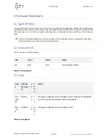
There is one LED on TE0714 module.
LED
Color
FPGA
Notes
D4
Red
K18
User programmable
Table 5: LED connection.
6.3 Clock
Cloc
k
Default
Frequen
cy
I
C
F
P
G
A
Notes
CLK
25M
Hz
25 MHz
U
8
T
1
4
Frequency depends on the module variant. Output is compatible
to 3.3V and 1.8V I/O standard of the FPGA bank.
MGT
_CL
K
125MHz
U
2
B
6/
B
5
Frequency depends on the module variant
Table 6: Clock signals.
SPI Flash QE (Quad Enable) bit must be set to high or FPGA is unable to load its configuration from flash.
By default this bit is set to high at the manufacturing plant.


