TE0714 TRM
Revision: v.55
Copyright © 2019 Trenz Electronic GmbH
9 of 22
http://www.trenz-electronic.de
1
https://shop.trenz-electronic.de/de/Download/?path=Trenz_Electronic/Pinout
5 Signals, Interfaces and Pins
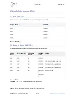
5.1 JTAG Interface
JTAG access to the Xilinx Artix-7 FPGA
device is
provided through connector
JM1.
Signal Name
B2B Pin
TCK
JM1:89
TDI
JM1:85
TDO
JM1:87
TMS
JM1:91
Table 3: JTAG signals.
5.2 Board to Board (B2B) I/Os
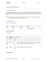
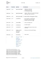
FPGA bank number and number of I/O signals connected to the B2B connector:
FPGA
Bank
B2B Connector
I/O Signal
Count
Voltage
Level
Notes
14
JM1
6
VCCIO_0
14
JM2
36
VCCIO_0
NB! 17 LVDS pairs possible.
15
JM2
48
VCCIO15
Supplied by the baseboard.
34
JM1
48
VCCIO34
Supplied by the baseboard.
216
JM1
16
MGT_AVC
C
MGT_AVT
T
4 x GTP lanes.
Table 4: B2B I/Os
Please refer to
the
Pin-out
1
tables page for additional information.


