background image

T6600C, T6600C/CD, T6600C/CDV

4-35

4.17 FDD

Removing the FDD

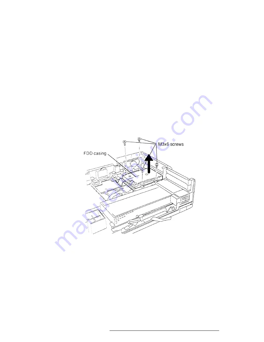
To remove the computer’s FDD, follow the steps below and refer to Figures 4-31 and 4-32.

1.

Turn off the power to the computer, then disconnect the power cord and all
external cables connected to the computer.

2.

Remove the optional PCMCIA card, optional memory card(s), keyboard unit,
optional turbo cache memory module, back cover, optional expansion card,
bottom cover, HDD, 5.25-inch bay (T6600C) or CD-ROM drive (T6600C/CD and
T6600C/CDV), back panel board, DC fan unit, and system board as described in
Sections 4.2 through 4.5 and 4.7 through 4.15.

3.

Remove the 

four M3x6 screws

 securing the 

FDD casing

, then lift out the 

FDD

with its 

casing

 (Figure 4-31).

Figure 4-31  Removing the FDD Unit

Summary of Contents for T-Series T6600c

Page 1: ... inch Floppy Disk Drive FDD supports 2HD floppy disks 1 44 Mbytes and 2DD floppy disks 720 Kbytes The T6600C also has a built in 5 25 inch bay for an optional CD ROM Memory The T6600C comes standard with 8 MB of CMOS Random Access Memory RAM This includes 640 KB of conventional memory and 7 424 KB of extended memory which can be utilized as a BIOS ROM data copy area and as expanded memory that is ...

Page 2: ...ory card slots 88 pin enable you to install the following Toshiba optional memory cards 4 MB memory card PA2004U 8 MB memory card PA2005U 16 MB memory card PA2010U Personal Computer Memory Card International Association PCMCIA card slot The optional built in PCMCIA slot measures 16 mm high Parallel port The Centronics compatible parallel interface port serves two purposes the port can be used to c...

Page 3: ...00C has a Small Computer System Interface SCSI port Audio ports The computer has the following standard 3 5 mm diameter miniature stereo jacks for an audio system Headphone with speaker shut off switch Line out Line in Microphone Special ports The T6600C has a Feature connector and Z connector for use with expansion cards ...

Page 4: ... T6600C CD T6600C CDV The T6600C Personal Computer is shown in Figure 1 1 and its system configuration is illustrated in Figure 1 2 Figure 1 1 T6600C Personal Computer Figure 1 2 T6600C System Unit Configuration ...

Page 5: ...T6600C T6600C CD T6600C CDV 1 5 1 2 System Unit Block Diagram Figure 1 3 shows a block diagram of the T6600C system unit Figure 1 3 T6600C System Board Block Diagram ...

Page 6: ...ps Memory card 4 8 or 16 MB memory card can be installed 32 bit data width Super Integration SI T9901 which stores the following components Two Direct Memory Access Controllers DMAC 82C37 equivalent Two Programmable Interrupt Controllers PIC 82C59 equivalent One Programmable Interval Timer PIT 82C54 equivalent One Floppy Disk Controller FDC TC8565 equivalent One Serial Input Output Controller SIO ...

Page 7: ...sly SCSI Controller An AIC6260 chip controls the internal Small Computer System Interface SCSI port Sound Controller An AD1848 chip controls the internal sound system The Clock Generator receives 14 31818 MHz X1 and generates the following frequencies 66 MHz for the CPU 14 7456 MHz for the COM 24 MHz for the FDC and VFO 16 MHz is used for KBC 8 MHz 14 31818 MHz for VGA display controller OSC X3 ge...

Page 8: ...This gate array has the following functions PCMCIA Card Interface control HDD and FDD access control by security register Communication control between system and KBC EEPROM access SCSI interrupt control External SIO control Sound system control Display type determine DAC digital output on off control Display signal on off control Back light on off control Feature connector and Z connector connect...

Page 9: ... and its specifications are described in Table 1 1 Figure 1 4 3 5 inch FDD Table 1 1 3 5 inch FDD Specifications Item 2 MB Mode 1 MB Mode Storage capacity KB Unformatted 2 000 1 000 Formatted 1 440 720 Number of heads 2 2 Number of cylinders 80 80 Access time ms Track to track 3 3 Average 181 181 Head settling time 15 15 Recording track density tpi 135 135 Data transfer rate Kbps 500 250 Rotation ...

Page 10: ... 1 5 and its specifi cations are described in Table 1 2 Figure 1 5 3 5 inch HDD Table 1 2 3 5 inch HDD Specifications Item Specification Model Name CP30544 Storage capacity MB Formatted 510 0 Number of disks 3 Data heads 6 Data surfaces 6 Tracks per surface 2243 Sectors per track 59 60 to 89 90 Bytes per sector 512 to 520 Access time ms Track to track 2 Average 10 Maximum 18 Rotation speed rpm 5 4...

Page 11: ... 102 key European keyboard is mounted on the T6600C s system unit and is connected to the keyboard controller on the system board through a 19 pin flat cable The keyboard is shown in Figure 1 6 See Appendix F for optional keyboard configurations Figure 1 6 Keyboard ...

Page 12: ...ons of the Video Graphics Array VGA The LCD receives vertical and horizontal synchronizing signals 9 bit data signals data enable signals and shift clock for data transmission All signals are CMOS level compatible The TFT LCD and FL inverter board are shown in Figure 1 7 and specifications for the LCD are described in Table 1 3 Figure 1 7 TFT Color LCD and FL Inverter Board Table 1 3 TFT Color LCD...

Page 13: ...gh frequency current to the LCD s Fluorescent Lamp Specifications for the FL inverter are described in Table 1 4 Table 1 4 FL Inverter Board Specifications Item Specifications Input Voltage VDC 24 Power W 12 5 Output Voltage VAC 1 100 r m s Current mA 7 mA r m s Frequency KHz 36 Current limits mA 5 0 to 7 0 ...

Page 14: ...iquid crystal display LCD 7 Option slots 8 DC fans 9 PS 2 mouse port The power supply unit includes an input line filter line fuse cooling fan power conversion circuitry and connectors Input ratings are 115 VAC 3 5 A or 230 VAC 1 7 A The power supply unit is shown in Figure 1 8 and the output ratings are specified in Table 1 5 Figure 1 8 Power Supply Unit Table 1 5 Power Supply Unit Output Rating ...

Page 15: ...wo Phillips screwdrivers 3 mm and 2 mm 3 A Toshiba MS DOS system disk s 4 A 2DD or 2HD formatted work disk for floppy disk drive testing 5 A cleaning kit for floppy disk drive troubleshooting 6 A printer port LED 7 An RS 232 C wraparound connector 8 A printer wraparound connector 9 A multimeter 10 An external 5 25 inch floppy disk drive 11 An external CRT 12 MS Windows V3 1 system disk 13 MS Windo...

Page 16: ...er removing all optional devices if the T6600C is found to be operating properly then an optional device or a T6600C interface is causing the problem Check the following items For a memory card PCMCIA card turbo cache module and connected I O port devices check the T6600C with the optional device or with a wraparound board for the I O port using the test program If the T6600C works with no errors ...

Page 17: ...T6600C T6600C CD T6600C CDV 2 3 Figure 2 1 Troubleshooting Flowchart 1 2 ...

Page 18: ...hooting procedures as follows 1 If an error is detected on the System Test Memory Test Display Test ASYNC Test Printer Test or Real Timer Test perform the System Board Troubleshooting Procedures in Section 2 4 2 If an error is detected on the Keyboard Test perform the Keyboard Troubleshoot ing Procedures in Section 2 7 3 If an error is detected on the Floppy Disk Test perform the Floppy Disk Drive...

Page 19: ...ed correctly go to Check 2 Check 2 Disconnect the power cord from the T6600C Use a multimeter to check the output voltage from the wall outlet on the power cord If the output voltage is not correct replace the power cord with a new one If output voltage is correct perform Procedure 2 Procedure 2 Connector Check The power supply cables should be connected to the system board These cables may be dis...

Page 20: ...connect the AC cord and turn on the power Use a multimeter to check the following voltages Table 2 1 Output Voltages Connector Pin No Voltage V PJ440 1 GND 2 5 10 3 GND 4 GND 5 GND 6 GND 7 GND 8 GND 9 GND 10 GND 11 12 10 PJ441 1 5 5 2 5 5 3 5 5 4 5 5 5 5 5 6 5 5 7 24 8V 4V 8 12 5 9 12 5 10 12 5 If the output voltages are not correct replace the power supply unit If the output voltages are correct ...

Page 21: ...ioning properly Start with Procedure 1 and continue with the other procedures as instructed The procedures described in this section are Procedure 1 Message Check Procedure 2 Printer Port LED Check Procedure 3 Diagnostic Test Program Execution Check Procedure 4 SCSI Logic Check Procedure 5 Sound Logic Check Procedure 6 System Board Replacement Check ...

Page 22: ...en press F1 key These errors occur when the system configuration preserved in the RTC memory CMOS type memory is not the same as the actual configuration or when data is lost If you press the F1 key as the message instructs the system configuration in the RTC memory configuration is set to the default setting If Error Message b appears often when the power is turned on replace the RTC battery If a...

Page 23: ...TC ERROR 9 RTC UPDATE ERROR 10 CRTC ERROR 11 VRAM ERROR 12 KBC ERROR 13 SYSTEM MEMORY ERROR 14 SYSTEM MEMORY PARITY ERROR 15 EXTENDED MEMORY ERROR 16 EXTENDED MEMORY PARITY ERROR 17 PROTECTED MODE ERROR 18 CPU EXCEPTION ERROR 19 DMA PAGE REGISTER ERROR 20 DMAC 1 ERROR 21 DMAC 2 ERROR 22 PIC 1 ERROR 23 PIC 2 ERROR 24 KEYBOARD ERROR 25 KBC ERROR 26 HDC ERROR 27 HDD 0 ERROR 28 HDD 1 ERROR 29 NO FDD E...

Page 24: ...T6600C s power 2 Plug the printer port LED into the computer s PRT FDD connector 3 Hold down the space bar and turn on the T6600C s power 4 Read the LED status from left to right as you face the back of the computer 5 Convert the status from binary to hexadecimal notation 6 If the final LED status is FFh normal status go to Procedure 3 7 If the final LED status matches any of the test status value...

Page 25: ...ation 0DH RTC test RTC ERROR READ DATA XXH WRITE DATA XXH RTC UPDATE ERROR 15H RTC initialization 16H PIC initialization 18H Display initialization CRTC ERROR VRAM ERROR READ DATA XXXXXXXXH WRITE DATA XXXXXXXXH 1FH KBC test KBC ERROR 22H System memory test SYSTEM MEMORY ERROR ADDRESS XXXXXXXXH READ DATA XXXXXXXXH WRITE DATA XXXXXXXXH SYSTEM MEMORY PARITY ERROR ADDRESS XXXX0000H XXXXFFFFH 25H Exten...

Page 26: ...test KEYBOARD ERROR 54H KBC initialization KBC ERROR 55H Mouse initialization 5BH Password check 5DH HDD initialization HDC ERROR HDC 0 ERROR HDC 1 ERROR 60H FDD initialization NO FDD ERROR FDD ERROR 65H Printer test 70H SIO test 80H Timer initialization TIMER INTERRUPT ERROR RTC UPDATE ERROR 90H NDP initialization A0H Expansion I O ROM A6H Others H W initialization FEH Expansion system ROM FFH CM...

Page 27: ... Section 2 7 Check 3 If Error Code 5Dh is displayed go to the HDD Troubleshooting procedures in Section 2 6 Check 4 If Error Code 60h is displayed go to the FDD Troubleshooting procedures in Section 2 5 Procedure 3 Diagnostic Test Program Execution Check Execute the following tests from the Diagnostic Test Menu Refer to Chapter 3 Tests and Diagnostics for more information on how to perform these t...

Page 28: ...to the external SCSI port PJ680 Step 5 Execute the HDD test of the diagnostic test program Select 2 HDD2 for the Test drive number If an error is detected during the HDD tests replace the system board with a new one Check 2 Internal SCSI interface check Step 1 Make sure the external SCSI port is not connected to PJ680 on the system board Step 2 Connect the internal SCSI HDD to PJ9 on the back pane...

Page 29: ...of the file run C SNDSYS SOUNDS POPJAZ30 RMI about line 90 of the file Step 4 Insert the following lines under sounds in the WIN INI file in the order indicated below SystemStart C SNDSYS SOUNDS WAGNER WAV Windows Start Step 5 Edit the AUTOEXEC BAT file as follows rem c DOS DOSSHELL change WIN add as the last line Preparation for the Test Step 1 Remove any SCSI devices that may be connected Be sur...

Page 30: ...click the Quick Recorder icon at the bottom left of the screen to display the Quick Recorder window Step 7 Click the red circle in the window and say test test into the mike to record your voice Step 8 Click the black square to stop recording Step 9 Click the black triangle to check that your voice is played back Step 10 Click the black square and select Options Step 11 Select Set Recording Level ...

Page 31: ... Board Replacement Check The system board may be damaged Disassemble the T6600C following the steps described in Chapter 4 Replacement Procedures and perform the following checks Check 1 Replace the system board with a new one Refer to Chapter 4 for instructions on how to remove and replace the unit If the problem still exists perform Check 2 Check 2 Replace the back panel board with a new one If ...

Page 32: ...er loading Toshiba MS DOS run the Diagnostic Program and then clean the FDD heads using the cleaning kit If the FDD still does not function properly after cleaning go to Proce dure 3 If the test program cannot be executed on the T6600C go to Procedure 2 Procedure 2 External 5 25 inch FDD Check The floppy disk controller on the computer s system board controls the internal and external FDD To deter...

Page 33: ...s are described in Table 2 4 Make sure the floppy disk in the FDD is formatted correctly and that the write protect tab is dis abled If any other errors occur while executing the FDD diagnostics test go to Procedure 4 Table 2 4 Floppy Disk Drive Error Codes and Statuses Code Status 01h Bad command 02h Address mark not found 03h Write protected 04h Record not found 06h Media removed on dual attach ...

Page 34: ... the keyboard cable cover Make sure the FDD cable is firmly connected to the system board FDD PJ290 System board If this cable is disconnected connect it to the system board and repeat Procedure 3 If the FDD is still not functioning properly perform Check 2 Check 2 The FDD or its cable may be defective or damaged Replace the FDD with a new one following the steps in Chapter 4 Replacement Procedure...

Page 35: ...er then perform the follow ing checks Check 1 Type C and press Enter If you cannot change to Drive C go to Check 2 If you can change to Drive C go to Procedure 2 Check 2 Type FDISK and press Enter Choose Display Partition Information from the FDISK menu If Drive C is listed go to Check 3 If Drive C is not listed return to the FDISK menu and choose the option to create a DOS partition on Drive C th...

Page 36: ...em disk in drive Press any key when ready or Non System disk or disk error Replace and press any key Check 3 Using the Toshiba MS DOS system disk install a system program on the hard disk using the SYS command If the following message appears on the display the system program has been transferred to the HDD Restart the T6600C If the error message still appears perform Check 4 System transferred Ch...

Page 37: ...ing message appears on the display the HDD is formatted Format complete If any other error message appears on the display refer to the Toshiba MS DOS Manual for more information and perform Check 2 Check 2 Using the T6600C Diagnostics disk format the HDD with a low level format option Refer to Chapter 3 Tests and Diagnostics for more information about the diagnostics program If the following messa...

Page 38: ...2h Bad address mark 04h Record not found 05h HDC not reset 07h Drive not initialized 08h HDC overrun DRQ 09h DMA boundary error 0Ah Bad sector error 0Bh Bad track error 10h ECC error 11h ECC recover enable 20h HDC error 40h Seek error 80h Time out error AAh Drive not ready BBh Undefined error CCh Write fault E0h Status error EEh Access time out error FFh Data compare error Check 1 Replace the HDD ...

Page 39: ... is functioning properly Procedure 2 Connector and Replacement Check The keyboard is connected to the system board cable This cable may be disconnected or damaged Disassemble the T6600C as described in Chapter 4 Replacement Procedures and perform the following checks Check 1 Remove the keyboard cable cover Make sure the keyboard cable is not damaged and is connected to the system board Keyboard un...

Page 40: ...l perform Procedure 2 Procedure 2 External CRT Check Connect the external CRT to the T6600C s external monitor port then boot the computer The computer automatically detects the external CRT If the external CRT works correctly the internal LCD display may be damaged Go to Procedure 3 If the external CRT appears to have the same problem as the internal LCD the display controller or connection betwe...

Page 41: ...so connected by a signal cable as shown below Any of these cables may be disconnected Disassemble the display unit and check the following cable connections Refer to Chapter 4 Replacement Procedures for more information about how to disassemble the computer FL inverter board CN 1 CN 2 CN 3 System board PJ630 CN 3 CN 2 CN 1 LCD module Figure 2 3 T6600C Display Connection If any of these cables are ...

Page 42: ...closed perform Check 4 Check 1 Replace the FL unit with a new one and test the display again If the problem still exists perform Check 2 Check 2 Replace the FL inverter board with a new one and test the display again If the problem still exists perform Check 3 Check 3 Replace the LCD module with a new one and test the display again If the problem still exists perform Check 4 Check 4 Replace the di...

Page 43: ... Module DIAGNOSTICS MENU and the Test Program Module DIAGNOSTICS TEST MENU The DIAGNOSTICS MENU consists of the following functions DIAGNOSTIC TEST HARD DISK FORMAT HEAD CLEANING LOG UTILITIES RUNNING TEST FDD UTILITIES SYSTEM CONFIGURATION SETUP The DIAGNOSTIC TEST option contains the following functional tests SYSTEM TEST MEMORY TEST KEYBOARD TEST DISPLAY TEST FLOPPY DISK TEST PRINTER TEST ASYNC...

Page 44: ...d connector 34M741621G01 for the RS 232 C port wrap around test ASYNC test An external SVGA display for the SVGA display test An optional memory card for the memory module test A PCMCIA wraparound card for the PCMCIA wraparound test A wraparound board for a 16 bit bus 34P711656G01 for the 32 bus wraparound test An RS 232 C direct cable for the point to point test ASYNC test An F Z special connecto...

Page 45: ...e Boot from Drive A 1 Insert a Toshiba operating system diskette into the floppy disk drive FDD 2 Turn on the computer then proceed to the Running the Diagnostics Program section Modify the CONFIG SYS File 1 Turn on the computer and allow it to boot 2 Deactivate the line in the CONFIG SYS file that loads the device driver for the expanded memory manager by using the DOS batch command REM You may a...

Page 46: ...NU 1 DIAGNOSTIC TEST 2 HARD DISK FORMAT 3 4 HEAD CLEANING 5 LOG UTILITIES 6 RUNNING TEST 7 FDD UTILITIES 8 SYSTEM CONFIGURATION 9 EXIT TO MS DOS 0 SETUP Select items Enter Specify Esc Exit NOTE To exit the T6600C DIAGNOSTIC TEST MENU press the Esc key If a test program is in progress press Ctrl Break to exit the test program or press Ctrl C to stop the program ...

Page 47: ...items Enter Specify Esc Exit Refer to Sections 3 4 through 3 14 for detailed descriptions of each Diagnostic Test 1 through 11 Function 88 sets the floppy disk drive and hard disk drive error retry count and Function 99 exits the submenus of the Diagnostic Test and returns to the Diagnostic Menu 4 Select the option you want to execute and press Enter The following message appears SYSTEM TEST XXXXX...

Page 48: ...rror is found and displays the operation guide on the right side of the display screen as shown below ERROR STATUS NAME HALT OPERATION 1 Test end 2 Continue 3 Retry These three selections have the following functions 1 Terminates the test program and exits to the subtest menu 2 Continues the test 3 Restarts the test from the beginning Use the arrow keys to move the cursor to the desired option and...

Page 49: ... pattern data 03 RAM refresh 04 Protected mode 05 Memory module 06 Cache memory 07 PCMCIA memory 08 Turbo cache memory 3 KEYBOARD 01 Pressed key display 101 02 Pressed key display 102 03 Pressed key code display 04 PS 2 Mouse 4 DISPLAY 01 VRAM write read 02 Character attributes 03 Character set 04 80 25 Character display 05 Graphics display color set 0 1 06 640 200 Graphics display 07 640 400 Grap...

Page 50: ... 02 Not used 03 Point to point send 04 Point to point receive 05 Not used 06 Interrupt test IRQ 4 3 5 8 HARD DISK 01 Sequential read 02 Address uniqueness 03 Random address data 04 Cross talk peak shift 05 Write read compare CE 06 Write specified address 07 Read specified address 08 ECC circuit 09 Sequential write 10 W R C specified address 9 REAL TIMER 01 Real time 02 Backup memory 03 Real time c...

Page 51: ...000h to FFFFFh 64KB Subtest 02 H W status This test reads and displays the hardware status as shown below 76543210 H W status 10101100 Bit7 Bit6 Bit5 Notch signal 2DD Bit4 FDD type 2MB Bit3 Bit2 Drive A B Ext A Bit1 External FDD OFF Bit0 Table 3 2 describes the hardware bit status for each bit tested Pressing Enter returns you to the subtest menu Table 3 2 Hardware Bit Status Bit H W Status 1 0 7 ...

Page 52: ...ored in the test program When the read information is lower than the reference data the test program displays the following screen image ROM BIOS V1 00 OK V1 10 SCC Version V1 26 NG V1 00 Reference data Current data When the read information is higher the display is unchanged To exit this screen press the S key Subtest 04 EEPROM ID check This subtest checks the EEPROM ID number through the KBC ...

Page 53: ...ntional memory 0 program end to 640 KB then reads the new data and compares the results with the original data Subtest 03 RAM refresh real mode This subtest writes a 256 byte unit of constant data to conventional memory 0 to 640 KB then reads the new data and compares the results with the original data The constant data is AAAAh and 5555h NOTE There is a short delay between write and read operatio...

Page 54: ...mber of miss hit Number of hit OK Number of miss hit Number of hit Fail Subtest 07 PCMCIA Memory NOTE To execute this test a PCMCIA memory card must be installed in the computer This subtest divides the PCMCIA window D0000h to DFFFFh into 64 KB increments It then executes the subtest by writing constant data to the PCMCIA memory reads the data and then compares it with the original data Subtest 08...

Page 55: ... When you execute this subtest the 101 key keyboard layout is drawn on the display When any key is pressed the corresponding key on the screen changes to an character Holding a key down enables the auto repeat function which causes the key s display character to blink Subtest 02 Pressed key display 102 NOTE The Num Lock and the Overlay mode must be off to execute this subtest When you execute this...

Page 56: ...ames are shown in Appendix E KEYBOARD TEST IN PROGRESS 302000 Scan code Character code Keytop Ins Lock Caps Lock Num Lock Scroll Lock Alt Ctrl Left Shift Right Shift PRESS Enter KEY Subtest 04 PS 2 mouse NOTE To execute the PS 2 mouse connect check a PS 2 mouse must be connected to the computer This subtest checks whether or not a PS 2 mouse is connected to the computer If this test does not detec...

Page 57: ...he video RAM and compared to the original data Subtest 02 Character Attributes modes 1 and 13h This subtest displays the following character attribute modes normal intensi fied reverse and blinking as shown in the display below The character attribute modes display the foreground color and intensified color 16 colors or 16 level gray scale using black blue red magenta green cyan yellow and white f...

Page 58: ...SPLAY TEST menu press Ctrl Break Subtest 03 Character Set In this subtest the character set addressed 00h to FFh is displayed in the 40 25 character mode as shown below Press Enter KEY To exit this subtest and return to the DISPLAY TEST menu press Ctrl Break 320 200 GRAPHICS DISPLAY 13 PRESS Enter KEY BLACK BLUE GREEN CYAN RED MAGENTA BROWN WHITE GRAY LIGHT BLUE LIGHT GREEN LIGHT CYAN LIGHT RED LI...

Page 59: ...LMNOPQRSTUVWXYZ _ abcdefghijklmnop 0123456789 ABCDEFGHIJKLMNOPQRSTUVWXYZ _ abcdefghijklmnopq 0123456789 ABCDEFGHIJKLMNOPQRSTUVWXYZ _ abcdefghijklmnopqr 0123456789 ABCDEFGHIJKLMNOPQRSTUVWXYZ _ abcdefghijklmnopqrs 0123456789 ABCDEFGHIJKLMNOPQRSTUVWXYZ _ abcdefghijklmnopqrst 0123456789 ABCDEFGHIJKLMNOPQRSTUVWXYZ _ abcdefghijklmnopqrstu 0123456789 ABCDEFGHIJKLMNOPQRSTUVWXYZ _ abcdefghijklmnopqrstuv 01...

Page 60: ...x400 Graphics Display modes 10 74 and 12 This subtest displays even dots odd dots and all dots in the 640x350 640x400 and 640x480 dot graphics modes 10 and 12 as shown below Pressing Enter changes the size of the displayed image To exit this subtest and return to the DISPLAY TEST menu press Ctrl Break 640 200 GRAPHICS DISPLAY X EVEN DOTS ODD DOTS ALL DOTS DRIVEN DRIVEN DRIVEN PRESS Enter KEY 640 X...

Page 61: ...HHHHHHHHHHHHHHHHHHHHHHHHHHHHHHHHHHHHHHHHHHHHH HHHHHHHHHHHHHHHHHHHHHHHHHHHHHHHHHHHHHHHHHHHHHHHHHH HHHHHHHHHHHHHHHHHHHHHHHHHHHHHHHHHHHHHHHHHHHHHHHHHH HHHHHHHHHHHHHHHHHHHHHHHHHHHHHHHHHHHHHHHHHHHHHHHHHH HHHHHHHHHHHHHHHHHHHHHHHHHHHHHHHHHHHHHHHHHHHHHHHHHH HHHHHHHHHHHHHHHHHHHHHHHHHHHHHHHHHHHHHHHHHHHHHHHHHH HHHHHHHHHHHHHHHHHHHHHHHHHHHHHHHHHHHHHHHHHHHHHHHHHH HHHHHHHHHHHHHHHHHHHHHHHHHHHHHHHHHHHHHHHHHHHHHHHH...

Page 62: ...inal data Upon completion of the test the message OK displays then the screen returns to the subtest menu Subtest 11 TFT color display This subtest displays seven screens The first shows a 64 color band across the screen the next three screens display 64 gradations mode 13 of red green and blue successively and the last three display 256 gradations mode 5F of red green and blue Press Enter to chan...

Page 63: ... disk in the test drive to be tested and press Enter Media in Drive X mode 0 2DD 1 2D 2 2D 2HD 2DD 3 2HD 3 Select the track you want the test to start on and press Enter Simply pressing Enter sets the start track to zero Test start track Enter 0 dd 00 79 4 The floppy disk test menu will appear after you select the start track number Select the number of the subtest you want to execute and press En...

Page 64: ...he Diagnostic Test Menu Refer to Step 3 at the beginning of this section to set the start track Subtest 02 Sequential Read Write This subtest continuously writes data pattern B5ADADh to all the specified tracks selected in Subtest 01 The data is then read and compared to the original data Subtest 03 Random Address Data This subtest writes random data to random addresses on all tracks defined in Su...

Page 65: ...hannel number and press Enter to execute the selected subtest Subtest 01 Ripple Pattern This subtest prints characters for codes 20h through 7Eh line by line while shifting one character to the left at the beginning of each new line 0123456789 ABCDEFGHIJKLMNOPQRSTUVWXYZ _ abcdefghijklmno 0123456789 ABCDEFGHIJKLMNOPQRSTUVWXYZ _ abcdefghijklmnop 0123456789 ABCDEFGHIJKLMNOPQRSTUVWXYZ _ abcdefghijklmn...

Page 66: ...und connector must be connected to the computer s printer port The printer wraparound connector 34M741986G01 wiring diagram is described in Appendix G This subtest checks the output and bidirectional modes of the data control and status lines through the printer wraparound connector PRINTER TEST 1 THIS LINE SHOWS NORMAL PRINT 2 THIS LINE SHOWS DOUBLE WIDTH PRINT 3 THIS LINE SHOWS COMPRESSED PRINT ...

Page 67: ...t EVEN Data pattern 20h to 7Eh The following message will appear at the bottom of the screen when Subtests 01 03 04 and 05 are selected Channel 1 XXXXh Channel 2 XXXXh Channel 3 XXXXh Select the channel number 1 3 The serial I O port address is specified by the XXXXh number Select the serial port channel number and press Enter to start the subtest Subtest 01 Wraparound board NOTE To execute this s...

Page 68: ...e RS 232 C direct cable is described in Appendix G This subtest sends 20h through 7Eh data to the receive side then receives the sent data and compares it to the original data Subtest 04 Point to point Receive This subtest used with Subtest 03 described above receives the data from the send side then sends the received data Subtest 05 Not used Subtest 06 Interrupt Test IRQ 4 3 5 This subtest check...

Page 69: ...nd Refer to the Toshiba MS DOS manual for details 1 When you select the hard disk test from the DIAGNOSTIC TEST menu the following message appears Test drive number select 1 HDD 1 2 HDD 2 0 HDD1 2 2 Select the hard disk drive number to be tested and press Enter The following message appears HDC F W error retry 1 yes 2 no 3 This message is used to select the retry operation when the hard disk contr...

Page 70: ...is a sequential reading of all the tracks on the HDD starting at Track 0 When all the tracks on the HDD have been read the test starts at the maximum track and reads the tracks on the HDD sequentially back to Track 0 Subtest 02 Address Uniqueness This subtest writes unique address data to each sector of the HDD track by track The data written to each sector is then read and compared with the origi...

Page 71: ...DD Subtest 07 Read specified address This subtest reads data which has been written to a specified cylinder and head on the HDD Subtest 08 ECC circuit This subtest checks the Error Check and Correction ECC circuit functions of the specified cylinder and head on the HDD Subtest 09 Sequential write This subtest writes specified 2 byte data to all of the cylinders on the HDD Subtest 10 W R C specifie...

Page 72: ...urrent time XX XX XX Enter new date PRESS ENTER KEY TO EXIT TEST 2 If the current date is not correct input the correct date at the Enter new date prompt and press Enter The following prompt will appear Enter new time 3 If the current time is not correct input the correct time in 24 hour format Pressing Enter toggles between the time and the date To exit press Ctrl Break Subtest 02 Backup Memory T...

Page 73: ... time are erased This subtest checks the real time clock increments making sure the date and time are displayed in the following format Current date 01 01 1989 Current time 00 00 37 Pressing Enter displays the following Current date 12 31 1988 Current time 23 59 58 PRESS Enter KEY TO EXIT TEST Press Ctrl Break to exit ...

Page 74: ... and follow the directions on the screen The NDP test contains one subtest that tests the T6600C s NDP functions Move the highlight bar to Subtest 01 and press Enter Subtest 01 NDP test This test checks the following functions of the co processor Control word Status word Bus Addition Multiplication To exit press Ctrl Break ...

Page 75: ...t executes the tests listed in Table 3 3 Table 3 3 Expansion Test Wraparound Subtest F32BUS Sub Address Good Bad Contents 01 00001 F0 x0 OSC CLK ALE REF signal 02 00002 FA xx 8259 1 IRQ7 6 5 4 3 NMI 00002 F8 xx 8259 2 IRQ14 12 11 10 9 03 ch 0003 nn xx DMA 1 Channel 1 3 nn FF AA 55 00 EE 99 44 00 04 00004 00 FF xx Data line Caaaa bb bb Address line aaaa test address bbbb read data 06 00006 nn xx Me...

Page 76: ...d in Table 3 4 Table 3 4 Expansion Test PCMCIA Wraparound Subtest Sub Address Good Bad Contents 01 00001 nn xx Address line 00001 nn xx REG CE 1 CE 2 nn A0 90 80 00 02 00002 ww rr Data line ww write data rr read data 03 00003 Speaker line 04 00004 40 80 xx Wait line 40 XX 80 05 00005 nn xx Other lines BSY BVD1 nn 21 00 Subtest 04 SCSI interface This subtest reads the 0 cylinder on the HDD ...

Page 77: ... MEMORY 01 Parity Error 02 Protected Mode Not Changed 14 Memory Read Write Error DD Cache Memory Error KEYBOARD 03 Mouse Interface Error 04 DCBP Interface Error FLOPPY DISK 01 Bad Command 02 Address Mark Not Found 03 Write Protected 04 Record Not Found 06 Media Removed 08 DMA Overrun Error 09 DMA Boundary Error 10 CRC Error 20 FDC Error 40 Seek Error 60 FDD Not Drive Error 80 Time out Error EE Wri...

Page 78: ...Card Modem 34 Error Card Modem 36 No Dial Tone Card Modem HARD DISK 01 Bad Command Error 02 Bad Address Mark Error 04 Record Not Found 05 HDC Not Reset Error 07 Drive Not Initialized 08 Overrun Error 09 DMA Boundary Error 0A Bad Sector 0B Bad Track Error 10 ECC Error 11 ECC Recover Enable 20 HDC Error 40 Seek Error 80 Time out Error AA Drive Not Ready BB Undefined Error CC Write Fault E0 Status Er...

Page 79: ...15 0 Error 0A Address Data Line R W Error 0B I O CH Ready Line Error 0C I O CS16 Line Error 0D Power On Off Line Error 0E Master Line Error 0F DMAC 16 bit transfer Error 10 DMAC 16 bit T C Flag 0 Error 11 DMAC 16 bit transfer Last Error 12 DMAC 16 bit T C Flag 1 Error 13 Serial I O CS Line Error 14 MEM CS16 Line Error 0 15 MEM CS16 Line Error 1 16 Address Line A23 17 Error 17 Protected Mode Not Ch...

Page 80: ...ents of the HDC status register and error register are described in Tables 3 6 and 3 7 Table 3 6 Hard Disk Controller Status Register Contents Bit Name Description 7 BSY 0 HDC is busy Busy 1 HDC is ready 6 DRDY 0 Hard disk drive is not ready to accept commands Drive ready 1 Hard disk drive is ready 5 DWF 0 DWF error is not detected Drive write fault 1 Write fault condition occurred 4 DSC 0 The har...

Page 81: ...ror Uncorrectable 1 Uncorrectable data error has been detected 5 Not used 4 IDNF 0 Other Identification 1 There is no ID field in the requested sector 3 Not used 2 ABRT 0 Other Abort 1 Illegal command error or a drive status error occurred 1 TK00 0 The hard disk found Track 0 during a recalibrate command Track 0 1 The hard disk could not find Track 0 during a recalibrate command 0 Not used ...

Page 82: ...mand See the Toshiba MS DOS manual for details on using the BACKUP command 3 17 1 Function Description 1 All track FORMAT This option performs a low level format of all the tracks on the hard disk as listed in Table 3 8 below NOTE Before executing the All Track FORMAT option check for bad tracks using the Bad Track CHECK option or display a list of bad tracks on the HDD Table 3 8 Hard Disk Formatt...

Page 83: ... contents of the hard disk will be erased when this program is ex ecuted Before executing the function transfer the contents of the hard disk onto a backup system This can be done with the Toshiba MS DOS BACKUP command See the Toshiba MS DOS manual for details on using the BACKUP command Select TEST 2 and press Enter in the DIAGNOSTIC MENU to display the following menu DIAGNOSTICS HARD DISK FORMAT...

Page 84: ...gister prompt appears Enter the cylinder and head numbers of the bad tracks and press Enter Note that if there are no bad tracks pressing Enter alone is the same as executing an All Track Format as described in Item e below WARNING Current DISK data will be completely destroyed Press Bad cylinder number dddd key Press Bad head number dd key Enter the cylinder and head number in the format above in...

Page 85: ...icated in the screen prompt shown below Drive number select 1 1 2 2 Interleave number 1 1 8 Press Cylinder number dddd Press Head number dd Press Enter to return to the Hard Disk Format menu 4 Bad track CHECK This subtest reads the entire disk and displays a list of bad tracks The test is terminated in case of a bad track check error To initiate the subtest enter the drive number at the prompt sho...

Page 86: ...tions 1 Select Test 4 from the DIAGNOSTIC MENU and press Enter The following messages display DIAGNOSTICS FLOPPY DISK HEAD CLEANING VX XX Mount cleaning disk s on drive s Press any key when ready 2 Remove the Diagnostics Disk from the FDD then insert the cleaning disk and press Enter 3 When the cleaning start message appears the FDD head cleaning has begun 4 The display automatically returns to th...

Page 87: ...5 Error status STS 6 FDD HDD or memory address ADDR 7 Write data WD 8 Read data RD 9 HDC status HSTS 10 Error status name ERROR STATUS NAME 3 19 2 Operations 1 Select 5 and press Enter in the DIAGNOSTIC MENU to log error information into RAM or onto a floppy disk Error information displays in the following format XXXXX ERRORS CNT TS NAME PASS STS ADDR WD RD HSTS STATUS NAME 001 FDD 02 0000 103 000...

Page 88: ...previous page The 3 key returns to the Diagnostic Menu The 4 key erases all error log information in RAM The 5 key outputs the error log information to a printer The 6 key reads the log information from a floppy disk The 7 key writes the log information to a floppy disk 3 If an error retry OK condition occurs a capital R is placed at the beginning of the error status However it is not added to the...

Page 89: ...ork disk in the FDD If a work disk is not loaded an error will be generated during the FDD testing 1 Remove the diagnostics disk from the floppy disk drive and insert the work disk 2 Select 6 from the Diagnostic Menu and press Enter the following message displays Printer wraparound test Y N Selecting Y Yes executes the printer wraparound test A printer wraparound connector must be connected to the...

Page 90: ...es or No and press Enter The following message appears Mount the work disk s on the drive s then press Enter key Warning The contents of the disk s will be destroyed 5 This program executes continuously To terminate the program press Ctrl Break ...

Page 91: ...le density 48 67 5 TPI MFM mode 512 bytes 9 sectors track b 2DD Double sided double density double track 96 135 TPI MFM mode 512 bytes 9 sectors track c 2HD Double sided high density double track 96 135 TPI MFM mode 512 bytes 18 sectors track 2 COPY This program copies data from a source floppy disk to a target floppy disk 3 DUMP This program displays the contents of the floppy disk both the 3 5 i...

Page 92: ... Disk from the FDD insert the work disk and press any key The following message displays when the FDD format is executed FDD TYPE TRACK XXX FDD TYPE HEAD X FDD TYPE SECTOR XX Format start track head XXX X After the floppy disk is formatted the following message appears Format complete Another format 1 Yes 2 No e Typing 1 displays the message from Step c above Typing 2 returns the test to the DIAGN...

Page 93: ...Another copy 1 Yes 2 No e To copy another disk type 1 and the message from Step a displays again Entering 2 returns the test program to the DIAGNOSTIC MENU 4 DUMP program a When DUMP is selected the following message appears DIAGNOSTICS HARD DISK FLOPPY DISK DUMP VX XX Drive type select 1 FDD 2 HDD b Select a format type number If 2 is selected the program goes to Step e Select FDD number 1 A 2 B ...

Page 94: ...ts 7 Number of hard disk drives 8 Number of printer ports 9 Number of Math co processors 10 Extended Memory Size 3 22 2 Operations Select 8 from the DIAGNOSTIC MENU and press Enter to display the following system configuration SYSTEM CONFIGURATION BIOS ROM VERSION VX XX SCC VERSION VX XX 639 KB MEMORY COLOR GRAPH 80 Column 1 FLOPPY DISK DRIVE S 1 ASYNC ADAPTER 1 HARD DISK DRIVE S 1 PRINTER ADAPTER...

Page 95: ...2 Display device 3 LCD display mode 3 Hard disk 1 HDD 0 capacity 2 HDD 1 capacity 4 Power on password 5 COM PRT FDD 1 Serial port 2 External FDD PRT 3 Printer port type 6 Others 1 Processing speed 2 Cache 3 Turbo cache 4 Display auto off 5 Numlock Init state 6 Keyboard key layout 7 SCSI interrupt level 8 SCSI BIOS address 9 Sound I O address 10 System speaker T6600C T6600C CD T6600C CDV 3 53 ...

Page 96: ...layed accurately reflect your hardware configuration and no changes are necessary The screen displays the following message Exit without saving Y N Press Y The system returns to the Diagnostic menu T6600C SETUP Total 8192KB Base 640KB Extended 7424KB Shadow BIOS 128KB BIOS Ver Display Adapter VGA Compatible Display Device LCD LCD Display Mode Color HDD 0 Capacity 510MB HDD 1 No Drive Serial Port C...

Page 97: ...ual Reset NOTE The cursor which is bar shaped indicates which option is presently selected 1 Use the arrow keys to move the cursor between options You can also select each option group by pressing the character on the keyboard corresponding to the first character of the heading for each option group For example if you press D the cursor moves to the top of the DISPLAY option group 2 When the curso...

Page 98: ...by the computer You cannot change this value However if you set Hard RAM this value changes automatically c Extended Displays the amount of extended memory the T6600C has available You cannot change this value d Shadow BIOS The Setup program displays 128 KB of RAM which is reserved for the Shadow BIOS ROM This field displays the amount of the extended memory used for the shadow BIOS ROM You cannot...

Page 99: ... the display mode of the color LCD display is deter mined by the type of the CRT either monochrome or color and the setting for this option has no effect Color Displays in color mode with a maximum of 512 or 256K colors Default Monochrome Displays in the monochrome mode with some intensity levels of gray for the color LCD display 3 Hard Disk As you change the values for this option using the space...

Page 100: ... following message appears along with a beep sound indicating you must repeat the last two steps Entry Error Once the power on password is set the system configuration program displays Registered To reset the power on password perform the following steps a Press the Space bar or BkSp key The following prompt appears Password Enter the currently registered password The character string you enter is...

Page 101: ...mer has forgotten the password and you cannot start up the computer contact Toshiba Service at 1 800 999 4273 5 COM PRT FDD This Setup option controls communication levels for the serial port assignments of the FDD PRT port and operation of the printer port a Serial port This option sets the COM level COM1 or COM2 for the serial port The serial port interrupt level IRQ and I O port base address fo...

Page 102: ...a bi directional port The option is valid only when the PRT FDD connector is used for the printer that is the External FDD PRT option is set to Printer The printer port type setting depends on the printer or other parallel device s attached to the PRT FDD connector The options are Output Activates uni directional operation Bi directional Activates bi directional operation When a printer is connect...

Page 103: ...peed c Turbo cache This option shows whether the Turbo cache hardware is installed This status is automatically detected by the computer d Display auto off This option enables or disables the display automatic power off When automatic power off is enabled the duration is set to 30 min 30 min Enables display automatic power off The internal display is automatically powered off if you do not use the...

Page 104: ...rupt level This option selects the SCSI BIOS interrupt level IRQ9 IRQ10 IRQ11 Disabled h SCSI BIOS address This option selects the starting address of the BIOS for SCSI devices 0C8000H 0CFFFFH 0D8000H 0DFFFFH 0E0000H 0EFFFFH Disabled i Sound I O base address This option selects the Sound I O base address 0530H 0604H 0E80H Disabled j System speaker This option enables or disables the system speaker...

Page 105: ...Display Mask Optional Memory Card FL Inverter Board Keyboard Unit LCD Module Optional Turbo Cache FL Unit Memory Keyboard Back Cover Optional Expansion Card Bottom Cover HDD 5 25 inch Bay CD ROM Drive Back Panel Board DC Fan Unit System Board Connector Board RTC Battery FDD Speakers Volume Board Power Supply Unit LED Board Before You Begin Look over the procedures in this section before you begin ...

Page 106: ...d in the corresponding figures 9 The T6600C contains many sharp edges and corners so be careful not to injure yourself 10 After you have replaced an FRU make sure the computer is functioning properly by performing the appropriate test on the FRU you have fixed or replaced Disassembly Procedures The T6600C has two basic types of cable connectors Pressure Plate Connectors Normal Pin Connectors To di...

Page 107: ...or the head of the screw and may prevent proper seating of an FRU After installing an FRU confirm that it and the computer are functioning properly Tools and Equipment The use of ElectroStatic Discharge ESD equipment is very important for your safety and the safety of those around you Proper use of these devices will increase the success rate of your repairs and lower the cost for damaged or destr...

Page 108: ...urn off the power to the computer then disconnect the power cord and all external cables connected to the computer 2 Turn the computer so the left side faces you 3 Locate the PCMCIA slot cover and slide it up to expose the PCMCIA card Figure 4 1 Figure 4 1 Opening the PCMCIA Slot Cover 4 Slide the release lock button downward to recess the metal tab Figure 4 2 Figure 4 2 The PCMCIA Slot ...

Page 109: ...lide the PCMCIA slot cover up to expose the PCMCIA slot Figure 4 1 2 Make sure the metal tab is fully recessed by sliding the release lock button all the way down Figure 4 2 3 Insert the PCMCIA card into the slot When the card is almost all the way into the slot push gently but firmly to ensure a firm connection with the computer Do not force the card into position 4 To prevent accidental ejection...

Page 110: ...d to the computer 2 Turn the computer so the left side faces you 3 Remove the optional PCMCIA card as described in Section 4 2 4 Locate the memory expansion slot cover and open it by sliding it down Figure 4 4 Figure 4 4 Opening the Memory Expansion Slot Cover 5 Grasp the memory card and pull it out If a second card is in the slot remove it also CAUTION To avoid damaging the memory card DO NOT tou...

Page 111: ...y expansion slots You may install the memory card in either slot As you insert the card guides in the slot lead the card into the socket 3 When the card is almost all the way in the slot push firmly but gently to ensure a firm connection with the computer Do not force the card into position 4 Close the memory expansion slot cover 5 Install the optional PCMCIA card as described in Section 4 2 6 Con...

Page 112: ...d to the computer 2 Remove the optional PCMCIA card and memory card s as described in Sections 4 2 and 4 3 3 Open the display panel Display latches are located on both the right and left sides of the liquid crystal display LCD panel 4 Lift out the keyboard unit and place it in front of the computer Figure 4 5 5 Remove the two screw covers then remove the two M3x6 screws Figure 4 5 6 Lift off the k...

Page 113: ...nstall the keyboard unit follow the steps below and refer to Figures 4 5 and 4 6 1 Connect the keyboard cable to PJ190 on the system board Figure 4 6 2 Route the keyboard cable as illustrated in Figure 4 6 3 Set the keyboard connector cover in place and secure it with two M3x6 silver screws Figure 4 5 4 Press the two screw covers into place Figure 4 5 5 Place the keyboard unit onto the computer 6 ...

Page 114: ...ter 2 Remove the keyboard connector cover as described in Section 4 4 3 Remove the turbo cache memory module from the turbo cache memory socket on the system board Figure 4 7 Turbo Cache Memory Module Installing an Optional Turbo Cache Memory Module To install a turbo cache memory module in the T6600C follow the steps below and refer to Figure 4 7 1 Install the memory module into the turbo cache m...

Page 115: ...isconnect the power cord and all external cables connected to the computer 2 Remove the optional PCMCIA card optional memory card s keyboard unit and optional turbo cache memory module as described in Sections 4 2 through 4 5 3 Turn the keyboard unit over and remove the eight M2 5x6 silver screws securing the bottom cover Figure 4 8 Figure 4 8 Removing the Keyboard 4 Remove the bottom cover from t...

Page 116: ...of the M2 5x4 screws Figure 4 9 Removing the Scan Controller Screws 7 Gently lift the scan controller board and rotate it in the direction of the arrow shown in Figure 4 9 8 Disconnect the keyboard interface cable from PJ11 and the keyboard cable from PJ10 on the scan controller board as shown in Figure 4 10 NOTE If you are replacing the keyboard cable it can be removed from the keyboard assembly ...

Page 117: ...re the silver side of the interface cable is facing up when you connect it Figure 4 10 3 Connect the keyboard cable to PJ10 on the scan controller board Figure 4 10 4 Place the scan controller board in the keyboard assembly as illustrated in Figure 4 9 Make sure the keyboard ground cable is installed under the screw next to the keyboard cable connection Secure the scan controller board with two M2...

Page 118: ...er 2 Remove the optional PCMCIA card optional memory card s keyboard unit and optional turbo cache memory module as described in Sections 4 2 through 4 5 3 Close the display panel turn the computer so the back faces you then turn it upside down 4 Remove the six M3x6 silver screws from the back cover 5 Open the top of the connector panel and remove the M3x6 silver screw located at the top center of...

Page 119: ... cover follow the steps below and refer to Figure 4 12 1 Place the back cover on the computer and secure it with seven M3x6 silver screws 2 Install the optional turbo cache memory module keyboard unit optional memory card s and optional PCMCIA card as described in Sections 4 5 through 4 2 ...

Page 120: ...d 4 7 3 Place the computer right side up with the back facing you 4 Remove the M3x6 screw that secures the expansion card to the computer NOTE When removing a Mambo card proceed to the section titled Removing a Mambo Card 5 Gently pull the expansion card out of the machine Figure 4 13 Removing an Expansion Card Removing a Mambo Card Refer to Figure 4 14 1 Gently pull the Mambo card out of the mach...

Page 121: ... feature connector cable to PJ581 and PJ580 on the system board Be sure to align the Z connector cable with the red stripe to the right and the feature connector cable with the red stripe to the left Note that the connectors on these cables are keyed for proper installation Figure 4 14 Figure 4 14 Mambo Card Cables and Connectors 2 Fit the right side of the expansion card into a pair of card guide...

Page 122: ...nnector and feature connector cables to P305 and P4 on the card Figure 4 14 Figure 4 16 Inserting an Expansion Card 4 Visually confirm that the connector and socket are aligned and push the card all the way into the socket with firm even pressure 5 Press firmly on both ends of the card This ensures that the connector fits securely into the expansion socket 6 Secure the expansion card with an M3x6 ...

Page 123: ...ional PCMCIA card optional memory card s keyboard unit optional turbo cache memory module back cover and optional expansion card as described in Sections 4 2 through 4 5 4 7 and 4 8 NOTE If you are going to be removing the system board proceed to Step 3 If you are going to be removing the 5 25 inch bay HDD or back panel board proceed to Step 4 3 Remove the two power supply cables from PJ440 and PJ...

Page 124: ...bottom cover follow the steps below and refer to Figures 4 17 and 4 18 1 Place the bottom cover on the computer and secure it with fourteen 14 M3x6 silver screws Figure 4 18 2 If the power supply cables and internal FDD cable are disconnected connect them to PJ440 PJ441 and PJ290 Figure 4 17 3 Install the optional expansion card back cover optional turbo cache memory module keyboard unit optional ...

Page 125: ...omputer 2 Remove the optional PCMCIA card optional memory card s keyboard unit optional turbo cache memory module back cover optional expansion card and bottom cover as described in Sections 4 2 through 4 5 and 4 7 through 4 9 3 Remove the four M3x6 screws securing the HDD unit Figure 4 19 4 Lift up the HDD and disconnect the HDD signal cable from PJ5 and the HDD power cable from PJ6 on the back p...

Page 126: ...power cable to the HDD Figure 4 20 2 Rotate the HDD power and signal cables between the HDD and the HDD casing Figure 4 20 3 Secure the HDD to the HDD casing with four HDD screws Figure 4 20 4 Connect the HDD signal cable to PJ5 and HDD power cable to PJ6 on the back panel board Figure 4 19 5 Place the HDD in the computer and secure it with four M3x6 screws Figure 4 19 6 Install the bottom cover o...

Page 127: ...al expansion card and bottom cover as described in Sections 4 2 through 4 5 and 4 7 through 4 9 3 Remove the three M3x6 screws securing the 5 25 inch bay and lift it out Figure 4 21 Removing the 5 25 inch Bay Installing the 5 25 inch Bay To install the T6600C s 5 25 inch bay follow the steps below and refer to Figure 4 21 1 Set the 5 25 inch bay in place and secure it with three M3x6 screws 2 Inst...

Page 128: ...e computer then disconnect the power cord and all external cables connected to the computer 2 Remove the optional PCMCIA card optional memory card s keyboard unit optional turbo cache memory module back cover optional expansion card bot tom cover and HDD as described in Sections 4 2 through 4 5 and 4 7 through 4 10 3 Remove the three M3x6 screws securing the CD ROM drive Figure 4 22 Figure 4 22 Re...

Page 129: ...or T6600C CDV s CD ROM drive follow the steps below and refer to Figures 4 22 and 4 23 1 Secure the CD ROM bracket to the drive with four M3x4 screws 2 Connect the audio cable to PJ362 on the system board 3 Connect the power cable to PJ7 on the back panel board 4 Connect the SCSI cable to PJ9 on the back panel board 5 Place the drive in the computer then connect the audio SCSI and power cables to ...

Page 130: ...rd optional memory card s keyboard unit optional turbo cache memory module back cover optional expansion card bottom cover HDD and 5 25 inch bay T6600C or CD ROM drive T6600C CD and T6600C CDV as described in Sections 4 2 through 4 5 and 4 7 through 4 12 3 Disconnect the DC fan cable from PJ8 on the back panel board and remove the two M3x6 screws securing the back panel frame Figure 4 24 4 Careful...

Page 131: ...k panel frame and secure it with six M3x6 screws Figure 4 25 2 Connect the back panel board to the system board at PJ490 and PJ491 then secure the board with two M3x6 screws Figure 4 24 3 Connect the DC fan cable to PJ8 on the back panel board Figure 4 24 4 Install the 5 25 inch bay T6600C or CD ROM drive T6600C CD and T6600C CDV HDD bottom cover optional expansion card back cover optional turbo c...

Page 132: ...l cables connected to the computer 2 Remove the optional PCMCIA card optional memory card s keyboard unit optional turbo cache memory module back cover optional expansion card bottom cover HDD 5 25 inch bay T6600C or CD ROM drive T6600C CD and T6600C CDV and back panel board as described in Sections 4 2 through 4 5 and 4 7 through 4 13 3 Remove the two M3x6 screws securing the DC fan unit and lift...

Page 133: ... unit in the computer and secure the unit with two M3x6 screws 2 Install the back panel board 5 25 inch bay T6600C or CD ROM drive T6600C CD and T6600C CDV HDD bottom cover optional expansion card back cover optional turbo cache memory module keyboard unit optional memory card s and optional PCMCIA card as described in Sections 4 13 through 4 7 and 4 5 through 4 2 ...

Page 134: ...computer 2 Remove the optional PCMCIA card optional memory card s keyboard unit optional turbo cache memory module back cover optional expansion card bottom cover HDD 5 25 inch bay T6600C or CD ROM drive T6600C CD and T6600C CDV back panel board and DC fan unit as described in Sections 4 2 through 4 5 and 4 7 through 4 14 3 Remove the two M3x6 screws and two M2 5x6 screws from the connector panel ...

Page 135: ...em Board Shield Plate 5 Disconnect the speaker cable from PJ390 and the volume cable from PJ380 located under the system board Figure 4 29 6 Disconnect the display cable by releasing the stopper from PJ630 then discon nect the pressure plate LED cable from PJ430 under the system board 7 Carefully lift out the system board Figure 4 29 Removing the System Board ...

Page 136: ... Connect the speaker cable to PJ390 and volume cable to PJ380 Figure 4 29 4 Set the system board shield plate in place and secure it with four M3x6 screws Figure 4 28 5 Set the connector panel board in place and secure it with two M3x6 screws and two M2 5x6 screws Figure 4 27 6 Install the DC fan unit back panel board 5 25 inch bay T6600C or CD ROM drive T6600C CD and T6600C CDV HDD bottom cover o...

Page 137: ...al memory card s keyboard unit optional turbo cache memory module back cover optional expansion card bottom cover HDD 5 25 inch bay T6600C or CD ROM drive T6600C CD and T6600C CDV back panel board DC fan unit and system board as described in Sections 4 2 through 4 5 and 4 7 through 4 15 3 Turn the system board over with the component side up and disconnect the RTC battery cable from PJ210 4 The RT...

Page 138: ...refer to Figure 4 30 1 Apply the double sided tape to the RTC battery then place the battery on the memory card slot of the system board 2 Connect the RTC battery cable to PJ210 3 Install the system board DC fan unit back panel board 5 25 inch bay T6600C or CD ROM drive T6600C CD and T6600C CDV HDD bottom cover optional expansion card back cover optional turbo cache memory module keyboard unit opt...

Page 139: ...2 Remove the optional PCMCIA card optional memory card s keyboard unit optional turbo cache memory module back cover optional expansion card bottom cover HDD 5 25 inch bay T6600C or CD ROM drive T6600C CD and T6600C CDV back panel board DC fan unit and system board as described in Sections 4 2 through 4 5 and 4 7 through 4 15 3 Remove the four M3x6 screws securing the FDD casing then lift out the ...

Page 140: ... the FDD casing and secure it with four M3x4 screws Figure 4 32 2 Place the FDD unit into the system unit and secure it with four M3x6 screws Figure 4 31 3 Install the system board DC fan unit back panel board 5 25 inch bay T6600C or CD ROM drive T6600C CD and T6600C CDV HDD bottom cover optional expansion card back cover optional turbo cache memory module keyboard unit optional memory card s and ...

Page 141: ...nd 4 7 through 4 15 3 Remove the two M3x6 screws securing each speaker and lift out the speakers 4 Remove the M3x6 screw securing the volume board and lift out the board Figure 4 33 Removing the Speakers and the Volume Board Installing the Speakers and Volume Board To install the speakers and the volume board follow the steps below and refer to Figure 4 33 1 Set the speakers into place and secure ...

Page 142: ... PCMCIA card optional memory card s keyboard unit optional turbo cache memory module back cover optional expansion card bot tom cover HDD 5 25 inch bay T6600C or CD ROM drive T6600C CD and T6600C CDV back panel board DC fan unit and system board as described in Sections 4 2 through 4 5 and 4 7 through 4 15 3 Remove the two M3x6 screws securing the expansion card support and lift it out 4 Remove th...

Page 143: ...r M3x6 screws 2 Set the expansion card support in place and secure it with two M3x6 screws 3 Install the system board DC fan unit back panel board 5 25 inch bay T6600C or CD ROM drive T6600C CD and T6600C CDV HDD bottom cover optional expansion card back cover optional turbo cache memory module keyboard unit optional memory card s and optional PCMCIA card as described in Sections 4 15 through 4 7 ...

Page 144: ...MCIA card optional memory card s keyboard unit optional turbo cache memory module back cover optional expansion card bot tom cover HDD 5 25 inch bay T6600C or CD ROM drive T6600C CD and T6600C CDV back panel board DC fan unit and system board as described in Sections 4 2 through 4 5 and 4 7 through 4 15 3 Disconnect the LED cable from PJ1 and the display switch cable from PJ2 on the LED board 4 Re...

Page 145: ...Connect the LED cable to PJ1 and the display switch cable to PJ2 on the LED board 3 Install the system board DC fan unit back panel board 5 25 inch bay T6600C or CD ROM drive T6600C CD and T6600C CDV HDD bottom cover optional expansion card back cover optional turbo cache memory module keyboard unit optional memory card s and optional PCMCIA card as described in Sections 4 15 through 4 7 and 4 5 t...

Page 146: ...w covers from the display hinges and the top corners of the display 3 Remove the four M3x6 silver screws from the display mask 4 Carefully insert your fingers between the mask and the LCD panel and pry open the latches Start with the four latches across the top of the display mask 5 Continue unlatching the mask along the sides four latches on each side and at the bottom two latches There is also a...

Page 147: ...ith the four latches in the display supports three in the larger support and one in the small support 2 Continue securing the latches along the bottom of the display two the sides four on each side and across the top four 3 Secure the display mask with four M3x6 silver screws at the display hinges and the top corners 4 Attach the screw covers at each display hinge and at the top corners of the dis...

Page 148: ...ribed in Section 4 21 3 Disconnect the two FL cables from CN 2 and CN 3 and the display cable from CN1 on the FL inverter board 4 Remove the three M3x6 screws securing the FL inverter board Figure 4 37 Removing the FL Inverter Board Installing the FL Inverter Board To install the FL inverter board follow the steps below and refer to Figure 4 37 1 Secure the FL inverter board with three M3x6 screws...

Page 149: ...l external cables connected to the computer 2 Remove the display mask as described in Section 4 21 3 Disconnect the two FL cables from CN2 and CN3 and the display cable from CN1 on the FL inverter board Figure 4 38 4 Remove the four M3x6 screws securing the LCD module to the LCD cover Figure 4 38 Note the ground cable secured by the bottom left screw 5 Carefully rotate the LCD module forward Figur...

Page 150: ...and 4 39 1 Place the LCD module face down on the front of the T6600C and connect the three display cables to CN 1 CN 2 and CN 3 on the LCD module Figure 4 39 2 Set the LCD module in the LCD cover and secure it with four M3x6 screws making sure to secure the ground cable with the bottom left screw Figure 4 38 3 Connect the FL cables to CN 2 and CN 3 and the display cable to CN 1 on the FL inverter ...

Page 151: ...off the power to the computer then disconnect the power cord and all external cables connected to the computer 2 Remove the display mask and LCD module as described in Sections 4 21 and 4 23 3 Lay the LCD module face down and use needle nose pliers to unbend the three latches holding the front and back frames together then lift the unit out of the front frame Figure 4 40 4 Remove the M2x4 silver s...

Page 152: ...ently unsnap the LCD panel at the corners from the FL unit and lift it off the panel Figure 4 42 CAUTION Be very careful when you unsnap the display panel If you use too much force you might break the panel s tabs 7 To separate the FL unit from the back frame remove the four M2x4 flat silver screws Figure 4 42 Figure 4 42 Removing the FL Unit from the Display Panel ...

Page 153: ...s to secure the snaps Figure 4 42 CAUTION Be very careful when you snap the display panel together If you use too much force you might break the panel s tabs 3 Secure the LCD panel to the FL unit with four silver M2x4 screws Figure 4 41 4 Place the assembly in the front frame and carefully bend the three latches back into place Figure 4 40 5 Secure the M2x4 silver screw to the cable side of the LC...

Page 154: ...e in the LCD cover be sure to seat it so that it is properly aligned and maximum visibility of the display is maintained 2 Be careful to align the holes at the four corners of the LCD module with the corresponding holes in the LCD cover before securing the module with screws Do not force the module into place because stress can affect its performance Also the panel s polarized surface is easily sc...

Page 155: ...rty we recommend a CRT cleaning agent Apply the agent to a cloth and then wipe the panel s surface Do not apply cleanser directly to the panel 4 If water or other liquid is left on the panel s surface for a long period it can change the screen s tint or stain it Be sure to quickly wipe off any liquid 5 Glass is used in the panel so be careful not to drop it or let it strike a hard object which cou...

Page 156: ...discharge Be sure to wear a wrist or ankle ground when handling the module 7 Do not expose the module to direct sunlight or strong ultraviolet rays for long periods 8 Do not store the module at temperatures below specifications Cold can cause the liquid crystals to freeze lose their elasticity or otherwise suffer damage ...

Page 157: ...mble the LCD module Disassembly can cause malfunctions 10 If you transport the module do not use packing material that contains epoxy resin amine or silicon glue alcohol or oxime These materials can release gas that can damage the panels polarization ...

Page 158: ...T6600C T6600C CD T6600C CDV B 1 Appendix B Board Layout B 1 T6600C System Board Front Figure B 1 T6600C System Board front ...

Page 159: ...B 2 T6600C T6600C CD T6600C CDV Figure B 2 T6600C System Board back ...

Page 160: ...tegration SI T9901 J IC 300 Serial Input Output SIO K IC 340 Sound Controller L IC 510 Video Controller WD90C31 M IC 520 Clock Generator N IC 540 to IC 543 Video Memory IC 550 to IC 553 Video Memory O IC 560 Display Timing Controller Gata Array P IC 570 Digital Analog Converter DAC Q IC 650 SCSI Controller R IC 660 SCSI BIOS S IC 10 Clock Generator 1 PJ 160 Memory Card Connector 2 PJ 190 Internal ...

Page 161: ...ble B 2 T6600C Connectors on the System Board back Mark Number Name A PJ 161 Memory Card Connector B PJ 380 Volume Connector C PJ 390 Speaker Connector D PJ 490 PJ 491 Back Panel Connector E PJ 581 Z Connector F PJ 580 Feature Connector ...

Page 162: ...05 111 O 16 MA04 111 O 60 MA07 111 O 17 VCC 61 MA09 111 O 18 MA06 111 O 62 GND 19 MA08 111 O 63 GND 20 MA10 111 O 64 GND 21 GND 65 RAS1 000 O 22 RAS0 000 O 66 CAS2 011 O 23 CAS0 011 O 67 GND 24 CAS1 011 O 68 CAS3 011 O 25 VCC 69 RAS3 000 O 26 RAS2 000 O 70 MWE 011 O 27 VCC 71 Pulled up 28 Pulled up 72 Not connected 29 Not connected 73 GND 30 Not connected 74 Not connected 31 Not connected 75 Not c...

Page 163: ...nected 61 MA09 111 O 18 MA06 111 O 62 GND 19 MA08 111 O 63 GND 20 MA10 101 O 64 GND 21 GND 65 RAS5 000 O 22 RAS4 000 O 66 CAS2 011 O 23 CAS0 011 O 67 GND 24 CAS1 011 O 68 CAS3 011 O 25 Not connected 69 RAS7 000 O 26 RAS6 000 O 70 MWE 011 O 27 VCC 71 Pulled up 28 Pulled up 72 Not connected 29 Not connected 73 GND 30 Not connected 74 Not connected 31 Not connected 75 Not connected 32 Not connected 7...

Page 164: ... O 27 GND 03 GND 28 SLIN 000 I O 04 FP 110 O 29 AUTFD 000 O 05 CGREEN 100 O 30 PINIT 000 O 06 CBLUE 100 O 31 GND 07 GND 32 STROB 000 O 08 CRED 100 O 33 PDB06 100 I O 09 GND 34 PDB07 100 I O 10 DCD1 111 I 35 GND 11 KBVCC 36 PDB05 100 O 12 SD1 011 O 37 PDB03 100 O 13 DSR1 111 I 38 PDB04 100 O 14 RD1 011 I 39 PCLR 100 O 15 GND 40 PDB02 100 O 16 DTR1 111 O 41 PDB00 100 O 17 RI1 111 I 42 PDB01 100 O 18...

Page 165: ...ctor 26 pin Table C 6 FDD Int Connector Pin Assignments 26 pin Pin Signal I O Pin Signal I O 01 VCC 14 ISTEP 000 O 02 INDEX 000 I 15 GND 03 VCC 16 IWDAT 000 O 04 IDSL 000 O 17 GND 05 VCC 18 IWEN 000 O 06 DSKCHG 000 I 19 GND 07 VCC 20 ITRO 000 I 08 IRDY 000 I 21 GND 09 IHMED 000 I 22 IWPR 000 I 10 IMON 000 O 23 GND 11 ILOWD 000 O 24 IRDAT 000 I 12 IDIRC 000 O 25 GND 13 GND 26 ISSEL 000 O ...

Page 166: ...nector Pin Assignments 3 pin Pin Signal I O Pin Signal I O 01 Right 03 Left I 02 GND C 7 PJ370 PJ381 PJ390 Audio Output Connectors Table C 10 PJ370 Line Out Connector Pin Assignments 3 pin Pin Signal I O Pin Signal I O 01 GND 03 Right O 02 Left O Table C 11 PJ381 Headphone Connector Pin Assignments 6 pin Pin Signal I O Pin Signal I O 01 GND 04 GND 02 Left O 05 PHONE I 03 Right O 06 Not connected T...

Page 167: ... T6600C CD T6600C CDV C 8 PJ380 Sound Gain Control Table C 13 PJ380 Volume Board Connector Pin Assignments 6 pin Pin Signal I O Pin Signal I O 01 LVOL 100 I 04 RVOL 100 I 02 LVOL 110 O 05 RVOL 110 O 03 GND 06 GND ...

Page 168: ...000 O 12 CADD08 100 O 46 CADD17 100 O 13 CADD13 100 O 47 CADD18 100 O 14 CADD14 100 O 48 CADD19 100 O 15 CWE 000 O 49 CADD20 100 O 16 CBSY 000 I 50 CADD21 100 O 17 MCVCCA 51 MCVCCA 18 MCVP1A 52 MCVP2A 19 CADD16 100 O 53 CADD22 100 O 20 CADD15 100 O 54 CADD23 100 O 21 CADD12 100 O 55 CADD24 100 O 22 CADD07 100 O 56 CADD25 100 O 23 CADD06 100 O 57 N C 24 CADD05 100 O 58 CRESET 100 O 25 CADD04 100 O ...

Page 169: ... 07 GND 04 Pulled up O 08 N C C 11 PJ440 PJ441 Power Supply Connectors Table C 16 PJ440 Power Supply Connector Pin Assignments 11 pin Pin Signal I O Pin Signal I O 01 GND 07 GND 02 M5V I 08 GND 03 GND 09 GND 04 GND 10 GND 05 GND 11 M12V I 06 GND Table C 17 PJ441 Power Supply Connector Pin Assignments 10 pin Pin Signal I O Pin Signal I O 01 VCC I 06 VCC I 02 VCC I 07 P24V I 03 VCC I 08 P12V I 04 VC...

Page 170: ... VCC 14 SD04 100 I O 54 IRQ5 100 I 15 DRQ2 100 I 55 SA08 100 I O 16 SD03 100 I O 56 IRQ4 100 I 17 GND 57 GND 18 SD02 100 I O 58 IRQ3 100 I 19 SD01 100 I O 59 DACK2 000 O 20 SD00 100 I O 60 TC 100 O 21 VCC 61 VCC 22 SMEW 000 O 62 BALE 100 O 23 AEN 100 O 63 14R3M 101 O 24 SMER 000 O 64 SBHE 000 I O 25 GND 65 GND 26 SA19 100 I O 66 LA23 100 I O 27 IOW 000 I O 67 IRQ10 100 I 28 SA18 100 I O 68 LA22 10...

Page 171: ...G 000 I O 15 DRQ7 100 I 55 P12V 16 SD12 100 I O 56 SCRST 000 O 17 GND 57 GND 18 SD13 100 I O 58 SCACK 000 I O 19 MASTER 000 I 59 P12V 20 SD14 100 I O 60 SCBSY 000 I O 21 VCC 61 P12V 22 SD15 100 I O 62 SCATN 000 I O 23 SA07 100 O 63 P12V 24 SA06 100 O 64 SCSIDP 000 I O 25 GND 65 GND 26 SA05 100 O 66 SCSID7 000 I O 27 SA04 100 O 67 P12V 28 SA03 100 O 68 SCSID6 000 I O 29 P12V 69 P12V 30 SA02 100 O 7...

Page 172: ...t connected 11 Not connected 24 FP 010 O 12 PVID5 010 O 25 Not connected 13 Not connected 26 GND Table C 21 PJ581 Z card Connector Pin Assignments 34 pin Pin Signal I O Pin Signal I O 01 DACR0 100 I 18 GND 02 DACR1 100 I 19 DACB0 100 I 03 GND 20 DACB1 100 I 04 DACR2 100 I 21 GND 05 DACR3 100 I 22 DACB2 100 I 06 GND 23 DACB3 100 I 07 DACR4 100 I 24 GND 08 DACR5 100 I 25 DACB4 100 I 09 GND 26 DACB5 ...

Page 173: ...ND 04 FLTLP 140 O 24 DATAG2 120 O 05 DATAR4 120 O 25 DATAB1 120 O 06 DATAR3 120 O 26 DATAB0 120 O 07 GND 27 DENAB 140 O 08 DATAR5 120 O 28 DATAB2 120 O 09 DATAG4 120 O 29 PNEL0 100 I 10 DATAG3 120 O 30 PNEL1 100 I 11 GND 31 GND 12 DATAG5 120 O 32 P24V O 13 DATAB4 120 O 33 LCDVCC O 14 DATAB3 120 O 34 P24V O 15 GND 35 GND 16 DATAB5 120 O 36 GND 17 DATAR1 120 O 37 LCDVCC O 18 DATAR0 120 O 38 FLOFF 10...

Page 174: ...30 GND 06 SCSID2 000 I O 31 GND 07 GND 32 SCATN 000 I O 08 SCSID3 000 I O 33 GND 09 GND 34 GND 10 SCSID4 000 I O 35 GND 11 GND 36 SCBSY 000 I O 12 SCSID5 000 I O 37 GND 13 GND 38 SCACK 000 I O 14 SDSID6 000 I O 39 GND 15 GND 40 SCRST 000 O 16 SCSID7 000 I O 41 GND 17 GND 42 SCMSG 000 I O 18 SCSIDP 000 I O 43 GND 19 GND 44 SCSEL 000 I O 20 GND 45 GND 21 GND 46 SCSICD 000 I O 22 GND 47 GND 23 GND 48...

Page 175: ...Appendix D USA Display Codes Table D 1 USA Display Codes T6600C T6600C CD T6600C CDV D 1 ...

Page 176: ...36 07 5E 07 36 07 5E 07 1E 7D 00 08 08 37 08 26 08 37 08 26 7E 00 7 08 37 08 26 08 37 08 26 7E 00 09 09 38 09 2A 09 38 09 2A 7F 00 8 09 38 09 2A 09 38 09 2A 7F 00 10 0A 39 0A 28 0A 39 0A 28 80 00 9 0A 39 0A 28 0A 39 0A 28 80 00 11 0B 30 0B 29 0B 30 0B 29 81 00 0 0B 30 0B 29 0B 30 0B 29 81 00 12 _ 0C 2D 0C 5F 0C 2D 0C 5F 0C 1F 82 00 0C 2D 0C 5F 0C 2D 0C 5F 0C 1F 82 00 13 0D 3D 0D 2B 0D 3D 0D 2B 83 ...

Page 177: ... 1A 5B 1A 7B 1A 1B 1A 00 28 1B 5D 1B 7D 1B 5D 1B 7D 1B 1D 1B 5D 1B 7D 1B 5D 1B 7D 1B 1D 1B 00 29 2B 5C 2B 7C 2B 5C 2B 7C 2B 1C 2B 5C 2B 7C 2B 5C 2B 7C 2B 1C 2B 00 30 Caps Lock 31 A 1E 61 1E 41 1E 41 1E 61 1E 01 1E 00 1E 61 1E 41 1E 41 1E 61 1E 01 1E 00 32 S 1F 73 1F 53 1F 53 1F 73 1F 13 1F 00 1F 73 1F 53 1F 53 1F 73 1F 13 1F 00 33 D 20 64 20 44 20 44 20 64 20 04 20 00 20 64 20 44 20 44 20 64 20 04...

Page 178: ...2E 63 2E 03 2E 00 49 V 2F 76 2F 56 2F 56 2F 76 2F 16 2F 00 2F 76 2F 56 2F 56 2F 76 2F 16 2F 00 50 B 30 62 30 42 30 42 30 62 30 02 30 00 30 62 30 42 30 42 30 62 30 02 30 00 51 N 31 6E 31 4E 31 4E 31 6E 31 0E 31 00 31 6E 31 4E 31 4E 31 6E 31 0E 31 00 52 M 32 6D 32 4D 32 4D 32 6D 32 0D 32 00 32 6D 32 4D 32 4D 32 6D 32 0D 32 00 53 33 2C 33 3C 33 2C 33 3C 33 2C 33 3C 33 2C 33 3C 33 00 54 34 2E 34 3E 34...

Page 179: ...D 00 4D 00 4D 00 74 00 4D E0 4D E0 4D E0 4D E0 74 E0 9D 00 110 Esc 01 1B 01 1B 01 1B 01 1B 01 1B 01 1B 01 1B 01 1B 01 1B 01 1B 01 00 112 F1 3B 00 54 00 3B 00 54 00 5E 00 68 00 3B 00 54 00 3B 00 54 00 5E 00 68 00 113 F2 3C 00 55 00 3C 00 55 00 5F 00 69 00 3C 00 55 00 3C 00 55 00 5F 00 69 00 114 F3 3D 00 56 00 3D 00 56 00 60 00 6A 00 3D 00 56 00 3D 00 56 00 60 00 6A 00 115 F4 3E 00 57 00 3E 00 57 00...

Page 180: ...5 Cap No Keytop Lower Upper Caps Lock Ctrl Alt Lower Upper 121 F10 44 00 5D 00 44 00 5D 00 67 00 71 00 44 00 5D 00 44 00 5D 00 67 00 71 00 122 F11 85 00 87 00 85 00 87 00 89 00 8B 00 123 F12 86 00 88 00 86 00 88 00 8A 00 8C 00 124 PrtSc 72 00 72 00 125 Scrl Lock 126 Pause 00 00 00 00 ...

Page 181: ...T6600C T6600C CD T6600C CDV F 1 Appendix F Key Layout F 1 United States US Keyboard Figure F 1 US Keyboard F 2 United Kingdom UK Keyboard Figure F 2 UK Keyboard ...

Page 182: ...F 2 T6600C T6600C CD T6600C CDV F 3 German GR Keyboard Figure F 3 GR Keyboard F 4 French FR Keyboard Figure F 4 FR Keyboard ...

Page 183: ...T6600C T6600C CD T6600C CDV F 3 F 5 Spanish SP Keyboard Figure F 5 SP Keyboard F 6 Italian IT Keyboard Figure F 6 IT Keyboard ...

Page 184: ...F 4 T6600C T6600C CD T6600C CDV F 7 Scandinavian SC Keyboard Figure F 7 SC Keyboard F 8 Swiss German SL Keyboard Figure F 8 SL Keyboard ...

Page 185: ...T6600C T6600C CD T6600C CDV F 5 F 9 Canadian Specialized Keyboard Figure F 9 Canadian Keyboard F 10 Keycap Number Keyboard Figure F 10 Keycap Number Keyboard ...

Page 186: ...SY Figure G 1 Printer Wraparound Connecter G 2 RS 232 C Wraparound Connector 3 TD 2 RD 7 RTS 8 CTS 1 CD 4 DTR 6 DSR 9 RI Figure G 2 RS 232 C Wraparound Connecter G 3 RS 232 C Direct Cable 9 pin to 9 pin 3 TD 2 RD 4 DTR 6 DSR 8 CTS 9 RI 7 RTS 1 CD 5 GND 5 GND 2 RD 3 TD 1 CD 7 RTS 6 DSR 4 DTR 8 CTS 9 RI Figure G 3 RS 232 C Direct Cable 9 pin to 9 pin T6600C T6600C CD T6600C CDV G 1 ...

Page 187: ...T6600C CD T6600C CDV G 4 RS 232 C Direct Cable 9 pin to 25 pin 1 CD 4 RTS 2 RD 2 TD 3 TD 3 RD 4 DTR 5 CTS 6 DSR 22 RI 5 GND 7 GND 7 RTS 8 CD 6 DSR 20 DTR 8 CTS 9 RI Figure G 4 RS 232 C Direct Cable 9 pin to 25 pin ...

Page 188: ...security reasons the Password Deletion Disk will not be distributed to Service Providers You must obtain the current password from the computer s owner to service the machine If the owner forgets the password contact your Toshiba representative for further action UPDATE ...

Page 189: ...OS Follow the procedures below to start the BIOS rewrite program 1 Turn off the power to the T6600C 2 Remove the external cable memory card and PCMCIA card 3 Turn on the power while holding down the F12 key Keep holding down the key until the system speaker sounds a beep 4 When the BIOS message is displayed insert the BIOS rewrite disk into the FDD Press the Enter key to start the BIOS rewrite pro...

Reviews: