

– 29 –
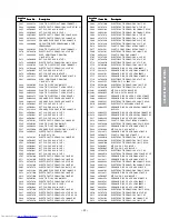
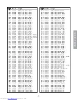
SPECIFIC INFORMATIONS
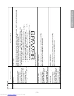
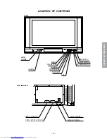
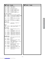
Location
Location
Location
Location
Location
Parts No.
Parts No.
Parts No.
Parts No.
Parts No.
Description
Description
Description
Description
Description
No.
No.
No.
No.
No.
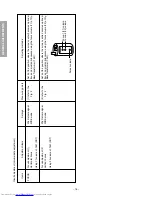
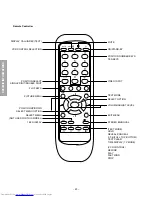
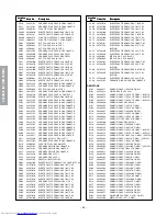
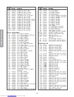
Location
Location
Location
Location
Location
Parts No.
Parts No.
Parts No.
Parts No.
Parts No.
Description
Description
Description
Description
Description
No.
No.
No.
No.
No.
Q4493
23314794
TRANSISTOR, VCEO=50V TO-92 2PC1815Y
Q451
23314794
TRANSISTOR, VCEO=50V TO-92 2PC1815Y
Q460
23314850
TRANSISTOR, 2SA1788, E
Q460B
72471082
SCREW, 3X10MM
Q461
23314794
TRANSISTOR, VCEO=50V TO-92 2PC1815Y
Q462
23314794
TRANSISTOR, VCEO=50V TO-92 2PC1815Y
Q470
23314794
TRANSISTOR, VCEO=50V TO-92 2PC1815Y
Q470
23114541
TRANSISTOR, 2SA1320
Q471
23314791
TRANSISTOR, VCEO=-50V TO-92 2PA1015Y
Q471
23314794
TRANSISTOR, VCEO=50V TO-92 2PC1815Y
Q472
23314794
TRANSISTOR, VCEO=50V TO-92 2PC1815Y
Q472
23314794
TRANSISTOR, VCEO=50V TO-92 2PC1815Y
Q473
23314791
TRANSISTOR, VCEO=-50V TO-92 2PA1015Y
Q490
23314794
TRANSISTOR, VCEO=50V TO-92 2PC1815Y
Q491
23314794
TRANSISTOR, VCEO=50V TO-92 2PC1815Y
Q501
B01A2479
IC, TB1251CN
Q511
23314794
TRANSISTOR, VCEO=50V TO-92 2PC1815Y
Q512
B0386235
YUV/RGB SW IC DIP 16 TA1287P
Q515
23314791
TRANSISTOR, VCEO=-50V TO-92 2PA1015Y
Q516
23314791
TRANSISTOR, VCEO=-50V TO-92 2PA1015Y
Q517
23314794
TRANSISTOR, VCEO=50V TO-92 2PC1815Y
Q518
23314794
TRANSISTOR, VCEO=50V TO-92 2PC1815Y
Q601
23114623
TRANSISTOR, 2SC2878-A(TEM
Q602
23114623
TRANSISTOR, 2SC2878-A(TEM
Q603
23114478
TRANSISTOR, RN2004
Q604
23314791
TRANSISTOR, VCEO=-50V TO-92 2PA1015Y
Q608
B0376856
IC, TA8211AH
Q612
23314794
TRANSISTOR, VCEO=50V TO-92 2PC1815Y
Q613
23314794
TRANSISTOR, VCEO=50V TO-92 2PC1815Y
Q618
23114623
TRANSISTOR, 2SC2878-A(TEM
Q619
23114623
TRANSISTOR, 2SC2878-A(TEM
Q671
23114623
TRANSISTOR, 2SC2878-A(TEM
Q673
23114623
TRANSISTOR, 2SC2878-A(TEM
Q701
23314791
TRANSISTOR, VCEO=-50V TO-92 2PA1015Y
Q705
23314794
TRANSISTOR, VCEO=50V TO-92 2PC1815Y
Q706
23314794
TRANSISTOR, VCEO=50V TO-92 2PC1815Y
Q707
23114437
TRANSISTOR, 2SC752GTM-Y
Q709
23314794
TRANSISTOR, VCEO=50V TO-92 2PC1815Y
Q710
23314791
TRANSISTOR, VCEO=-50V TO-92 2PA1015Y
Q711
A6550640
TRANSISTOR, 2SA1837
Q711B
70391355
SCREW, 3X8MM
Q712
A6369650
TRANSISTOR, 2SC4793
Q712B
70391355
SCREW, 3X8MM
Q719
23314794
TRANSISTOR, VCEO=50V TO-92 2PC1815Y
Q801
23135023
IC, HYBRID VDSS=800V STR-F6667B
Q801B
72471082
SCREW, 3X10MM
Q802
23314141
TRANSISTOR, 2SC3852
Q802B
70391355
SCREW, 3X8MM
Q805
23314794
TRANSISTOR, VCEO=50V TO-92 2PC1815Y
* Q826
23904427
IC, PHOTO COUPLER, TLP621(GR-LF2
Q827
23319693
IC, SE116N, LF4
Q840
23318299
IC, L78MR05-FA
Q840B
70391355
SCREW, 3X8MM
Q841
23314794
TRANSISTOR, VCEO=50V TO-92 2PC1815Y
Q842
23314794
TRANSISTOR, VCEO=50V TO-92 2PC1815Y
Q861
23314141
TRANSISTOR, 2SC3852
Q861B
70391355
SCREW, 3X8MM
Q901
A6363200
TRANSISTOR, 2SC3619
Q902
23314794
TRANSISTOR, VCEO=50V TO-92 2PC1815Y
Q903
A6363200
TRANSISTOR, 2SC3619
Q904
23314794
TRANSISTOR, VCEO=50V TO-92 2PC1815Y
Q905
A6363200
TRANSISTOR, 2SC3619
Q906
23314794
TRANSISTOR, VCEO=50V TO-92 2PC1815Y
Q907
23114422
TRANSISTOR, 2SA562TM-Y(T
Q908
23114429
TRANSISTOR, 2SC2120-Y(TE
Q4200
B01A0156
IC, PROCESSOR, TA1318N
QA01
23000703
IC, 8BIT TV/TEXT MCU 64K SAA5563PS/M3/
QA02
23905666
IC, 16384BITS AT24C1610PC
QA03
23114733
TRANSISTOR, 2SC2655-Y
QA04
23114458
TRANSISTOR, RN1206 (32Z13G)
QA05
23314794
TRANSISTOR, VCEO=50V TO-92 2PC1815Y
QB01
23314791
TRANSISTOR, VCEO=-50V TO-92 2PA1015Y
QB02
23314794
TRANSISTOR, VCEO=50V TO-92 2PC1815Y
QB30
23314791
TRANSISTOR, VCEO=-50V TO-92 2PA1015Y
QB30
23906946
IC, RAMDAC 3CH CM0016AD
QF01
23314794
TRANSISTOR, VCEO=50V TO-92 2PC1815Y
QR01
70129053
IC, SW 2IN 1OUT 3CIRCUIT ALLCLP BA7603
QR02
23114437
TRANSISTOR, 2SC752GTM-Y
QR03
23314794
TRANSISTOR, VCEO=50V TO-92 2PC1815Y
QR04
23114460
TRANSISTOR, RN1204
QR05
23114460
TRANSISTOR, RN1204
QV01
B0385655
IC, TA1219N
QV02
23314794
TRANSISTOR, VCEO=50V TO-92 2PC1815Y
QV03
23314791
TRANSISTOR, VCEO=-50V TO-92 2PA1015Y
QV04
23314794
TRANSISTOR, VCEO=50V TO-92 2PC1815Y
QV05
23114623
TRANSISTOR, 2SC2878-A(TEM
QV06
23114623
TRANSISTOR, 2SC2878-A(TEM
QV07
23114478
TRANSISTOR, RN2004
QV08
23314794
TRANSISTOR, VCEO=50V TO-92 2PC1815Y
QV11
23314791
TRANSISTOR, VCEO=-50V TO-92 2PA1015Y
D101
23115599
DIODE, 1N4148 (32Z13G)
D102
23357354
DIODE, MA2C858 (32Z13G)
D110
23357354
DIODE, MA2C858 (32Z13G)
D190
23316755
DIODE, ZENER VZ30.90-32.50 DO34
MTZ J 33C
D224
23115599
DIODE, 1N4148
D240
23115599
DIODE, 1N4148
D301
23118479
DIODE, BYD33J
D302
23118479
DIODE, BYD33J
D303
23316794
DIODE, SC570A
D304
23118479
DIODE, BYD33J
D308
23118479
DIODE, BYD33J
D312
23115599
DIODE, 1N4148
D320
23115599
DIODE, 1N4148
D327
23316717
DIODE, ZENER, MTZ J 11C
D336
23316672
DIODE, ZENER, MTZJ5.6B
D337
23316672
DIODE, ZENER, MTZJ5.6B
D370
23316658
DIODE, ZENER, MTZJ3.6A
D371
23115599
DIODE, 1N4148
D373
23316690
DIODE, ZENER, MTZJ10B
D374
23115599
DIODE, 1N4148
D377
23118479
DIODE, BYD33J
D378
23118479
DIODE, BYD33J
D401
23316685
DIODE, ZENER, MTZJ8.2C
D403
23115599
DIODE, 1N4148
D406
23118479
DIODE, BYD33J
D421
23316680
DIODE, ZENER, MTZJ7.5A
D422
23316726
DIODE, ZENER, MTZJ15C
D431
23316670
DIODE, ZENER, MTZJ5.1C
D432
23316670
DIODE, ZENER, MTZJ5.1C
D436
23115599
DIODE, 1N4148
D441
23316690
DIODE, ZENER, MTZJ10B
D4410
23115599
DIODE, 1N4148
D4411
23115599
DIODE, 1N4148
D4412
23115599
DIODE, 1N4148
D460
23118479
DIODE, BYD33J
D461
23316803
DIODE, VRSM=600V IF=5A FR 220FP
FMU-G16S
D461B
70391355
SCREW, 3X8MM
D463
23115599
DIODE, 1N4148
Summary of Contents for 32Z13B
Page 32: ... 32 SPECIFIC INFORMATIONS THIS PAGE IS INTENTIONALLY LEFT BLANK ...
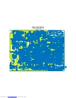
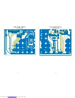
Page 33: ... 33 34 SIGNAL BOARD PD0015C SIGNAL BOARD PD0015D BOTTOM FOIL SIDE ...
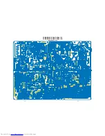
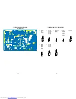
Page 34: ... 35 36 POWER DEF BOARD PD0016C POWER DEF BOARD PD0016D BOTTOM FOIL SIDE ...
Page 35: ... 37 38 CONT 1 BOARD PD0017A 1 BOTTOM FOIL SIDE CONT 2 BOARD PD0017A 2 BOTTOM FOIL SIDE ...
Page 37: ... 41 SPECIFIC INFORMATIONS MEMO ...
Page 38: ... 42 SPECIFIC INFORMATIONS MEMO ...
Page 40: ......