www.ti.com
Overview
1.4
Board Orientation
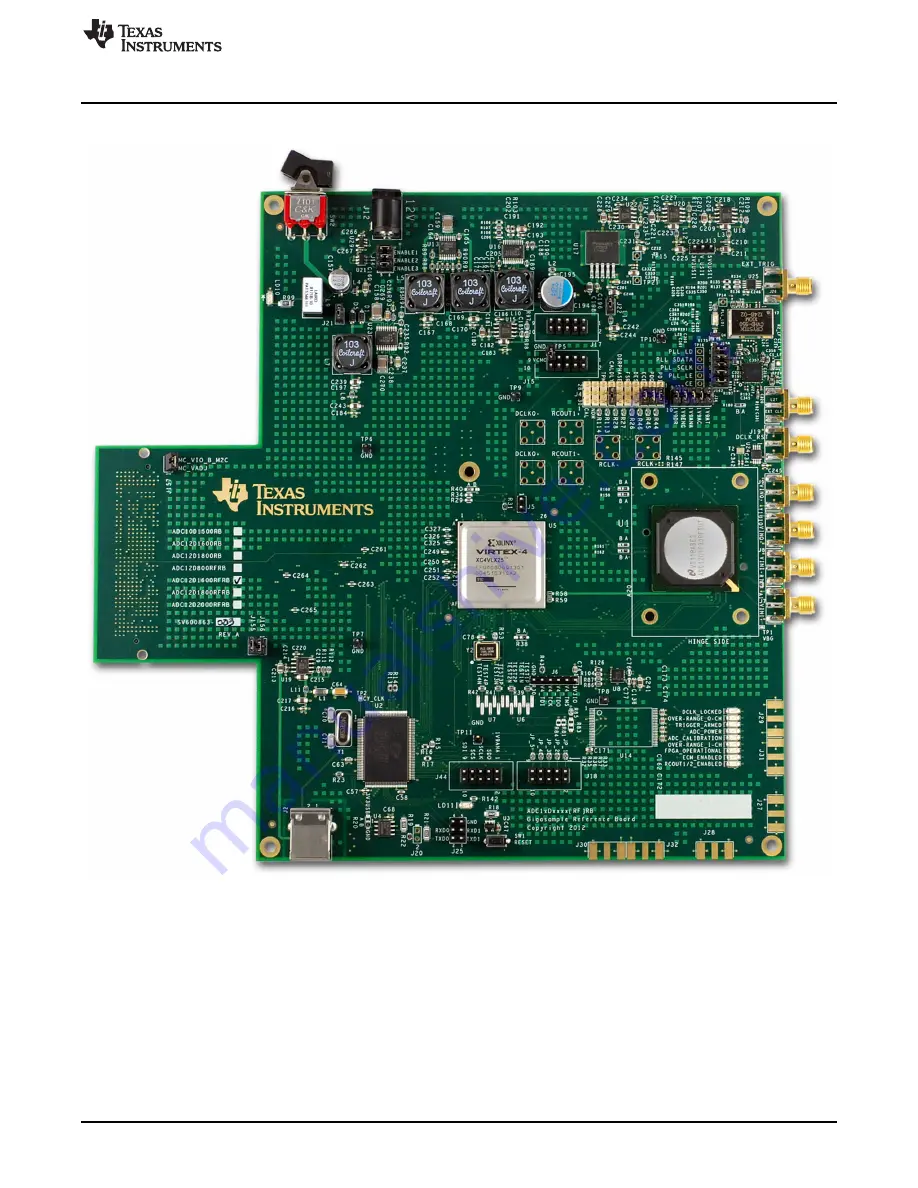
Figure 2. ADC1xDxxxx(RF)RB Board Layout
5
SNAU146 – September 2013
ADC1xDxxxx(RF)RB Reference Board
Submit Documentation Feedback
Copyright © 2013, Texas Instruments Incorporated
Page 1: ...ADC1xDxxxx RF RB Reference Board User s Guide Literature Number SNAU146 September 2013...
Page 2: ...family is pin compatible the same PCB is able to support the following devices ADC12D1800RF ADC12D1600RF ADC12D800RF ADC12D1800 ADC12D1600 ADC10D1500 In some cases the same board may be used to evalu...
Page 3: ...by the ADC 1 1 Features Demonstrates the ADC1xDxxxx RF s typical dynamic performance see the datasheet for full details Dual channel sample rates of up to 1 8 GS s limited by the ADC specifications a...
Page 4: ...ion can be found on the product web folder the Design Package contains FPGA source code schematic layout and BOM source files The WaveVision5 software may be downloaded for free from Texas Instruments...
Page 5: ...com Overview 1 4 Board Orientation Figure 2 ADC1xDxxxx RF RB Board Layout 5 SNAU146 September 2013 ADC1xDxxxx RF RB Reference Board Submit Documentation Feedback Copyright 2013 Texas Instruments Incor...
Page 6: ...close to the one shown in Figure 3 as possible This setup along with the board and software configuration described below is what was used to test the reference board at Texas Instruments lab This set...
Page 7: ...F 5 tunable bandpass filter or other fixed frequency bandpass filter of equivalent performance Balun ADC LD BB DC blocks Mini Circuits BLK 89 S 50 terminators Mini Circuits ANNE 50 Note The board come...
Page 8: ...ecked inside the Wavevision 5 GUI Does not clear upon data capture ADC_POWER Lights when ADC supply voltage of 1 9V is detected ADC_CALIBRATION Will light temporarily when calibration is run ADC s Cal...
Page 9: ...cess panels that are pertinent to the current plot window such as channel selection grid selection FFT Readouts and FFT controls The right side panels allow the user to take control of the hardware Th...
Page 10: ...s jumper in place This means that the ADC will be controlled through the SPI interface and not with jumpers driving the control pins This allows the user to control the ADC s behavior through the Wave...
Page 11: ...nabled only when an evaluation board which supports hardware histograms is attached 5 Acquire Data Click this button to acquire data to the active plot If you have created more than one plot the Activ...
Page 12: ...5 main window command buttons Open the Signal Source panel on the right side of the window and confirm that the ADC1xDxxxx RF RB is available and confirm that it is selected There are seven possible m...
Page 13: ...g and falling edge of the sample clock This effectively doubles the sample rate In this mode both converters inside the ADC12D1X00RF work on a common input signal The various DES modes are selected fr...
Page 14: ...FT bandwidth resolution but at the expense of more memory and slower acquisition time Data Format The default data format is offset binary for the ADC12D1X00RF FFT buffers to average The last option i...
Page 15: ...o double edge sampling DES For more information refer to the Calibration section of the ADC12D1X00RF datasheet The H W Trigger function is also enabled using the check box on this tab Note If the Inte...
Page 16: ...ked the device will continually output a fixed pattern on the Data and OR outputs When cleared the normal ADC Data and OR information are output PDI Power down I Channel when checked PDQ Power down Q...
Page 17: ...Calibration control via the SPI i e not the pin controlled option for calibration Note No changes will take effect until the Write Config Reg button is clicked I channel This tab changes the sign and...
Page 18: ...is also displayed in approximate mV I Channel Full Scale The approximate I Channel input full scale range mV peak to peak is selected ranging from a minimum of 600mV to a maximum of 1000mV The default...
Page 19: ...ouse pointer or using left right arrow keys once the slider has been selected Although the time skew is entered in 8 bit 0 to 127 relative form it is also displayed in approximate fs Note No changes w...
Page 20: ...perture Delay applied Fine Phase Adjust Sets the approximate amount of fine Aperture Delay applied SA Select tAD Adjust When checked enables the Aperture Delay Time fine adjust feature Overrides the S...
Page 21: ...Select Phase Selects the Phase of the incoming reference clock used by the AutoSync feature Reference Clock Delay This selects the additional delay added to the input reference clock Settings are 0d 0...
Page 22: ...of the Xilinx Virtex 4 FPGA Note No changes will appear until the Update Temperatures button is clicked Debug Tabs These panels provide the actual register settings which are conveniently formatted in...
Page 23: ...sub tab 2 6 1 Configure Display Settings Open the FFT Control left panel Confirm that the dBFS unit is selected Also confirm that the correct clock frequency is being measured by the software by chec...
Page 24: ...and pass filters similar to the items referenced in Section 2 2 should be used The absence of these filters on the input signal or external clock will usually result in sub standard performance The di...
Page 25: ...2 System Description 4 2 1 The ADC12D1X00RF ADC12D1X00RF forms the heart of this reference board This low power high performance CMOS analog to digital converter digitizes signals at 12 bit resolutio...
Page 26: ...the clock synthesis chip The clock source for the ADC can be selected between the on board LMX2541 or an external clock source connected through the J11 SMA connector The selection is performed throug...
Page 27: ...samples Figure 22 Trigger circuit on reference board 1 Connect a signal source to the EXT_TRIG SMA J26 2 In the WaveVision5 GUI select Registers Settings check the H W Trigger box 3 Select single or c...
Page 28: ...to FPGA Remove R162 R163 R158 R159 Route DCLKQ RCOUT1 RCLK to SMA connectors Stuff 0ohm resistors to R161 R164 R157 R160 R145 R147 Enable AutoSync output by going to Wavevision 5 Software GUI Register...
Page 29: ...an be monitored The temperature readings are available through the WV 5 software 5 Electrical Specifications Table 2 Electrical Specifications Nominal 12V Power Supply Minimum 11V Maximum 13V Voltages...
Page 30: ...ncy energy and has not been tested for compliance with the limits of computing devices pursuant to part 15 of FCC or ICES 003 rules which are designed to provide reasonable protection against radio fr...
Page 31: ...na type and its gain should be so chosen that the equivalent isotropically radiated power e i r p is not more than that necessary for successful communication This radio transmitter has been approved...
Page 32: ...roduct only after you obtained the license of Test Radio Station as provided in Radio Law of Japan with respect to this product or 3 Use of this product only after you obtained the Technical Regulatio...
Page 33: ...erations per the user guidelines Exceeding the specified EVM ratings including but not limited to input and output voltage current power and environmental ranges may cause property damage personal inj...
Page 34: ...sponsible for compliance with all legal regulatory and safety related requirements concerning its products and any use of TI components in its applications notwithstanding any applications related inf...