


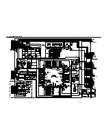

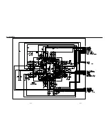


5. SCHEMATIC DIAGRAMS
5-2
5-1
SLV-D350P/D550P
◆
Block Identification of Main PCB - - - - - - - - - - - - - - - - - - - - - - - - - - - - - - - - 5-3
VCR Main PCB
5-1
S.M.P.S. - - - - - - - - - - - - - - - - - - - - - - - - - - - - - - - - - - - - - - - - - - - - - - 5-5
5-2
Power Drive - - - - - - - - - - - - - - - - - - - - - - - - - - - - - - - - - - - - - - - - - - - - 5-7
5-3
Logic/Function-Time - - - - - - - - - - - - - - - - - - - - - - - - - - - - - - - - - - - - - - 5-9
5-4
A/V - - - - - - - - - - - - - - - - - - - - - - - - - - - - - - - - - - - - - - - - - - - - - - - - - - 5-11
5-5
Hi-Fi/MTS - - - - - - - - - - - - - - - - - - - - - - - - - - - - - - - - - - - - - - - - - - - - - 5-13
5-6
Input-Output- - - - - - - - - - - - - - - - - - - - - - - - - - - - - - - - - - - - - - - - - - - - 5-15
DVD Main PCB
5-7
DVD - - - - - - - - - - - - - - - - - - - - - - - - - - - - - - - - - - - - - - - - - - - - - - - - - 5-17
Note
For schematic Diagram
- Resistors are in ohms, 1/8W unless otherwise noted.
Special note :
Most semiconductor devices are electrostatically sensitive and therefore require the special handling techniques described under the
“electrostatically sensitive (ES) devices” section of this service manual.
Important safety notices :
Components identified with the mark
0
have the special characteristics for safety. When replacing any of these components.
Use only the same type.
Summary of Contents for RMT-V501C
Page 10: ... 10 MEMO ...
Page 67: ...3 BLOCK DIAGRAM 3 2 3 1 SLV D350P D550P ...
Page 68: ...3 4E MEMO ...
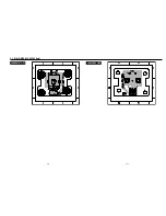
Page 70: ...4 3 4 4 4 1 VCR MAIN FUNCTION TIMER COMPONENT SIDE ...
Page 71: ...4 6 4 5 CONDUCTOR SIDE ...
Page 72: ...4 7 4 8 COMPONENT SIDE CONDUCTOR SIDE 4 2 DVD MAIN ...
Page 73: ...4 10 4 9 4 3 DIAL TIMER SLV D550P Only COMPONENT SIDE CONDUCTOR SIDE ...
Page 74: ...4 12E MEMO ...
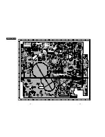
Page 76: ... BLOCK IDENTIFICATION OF MAIN PCB 5 3 5 4 Component Side Conductor Side VCR MAIN PCB ...
Page 77: ...5 1 S M P S 5 6 5 5 ...
Page 78: ...5 2 POWER DRIVE 5 7 5 8 ...
Page 79: ...5 3 LOGIC FUNCTION TIMER 5 10 5 9 ...
Page 80: ...5 4 A V 5 11 5 12 ...
Page 81: ...5 5 Hi Fi MTS 5 14 5 13 ...
Page 82: ...5 6 INPUT OUTPUT 5 15 5 16 ...
Page 83: ...5 7 DVD 5 18 5 17 ...
Page 84: ...MEMO 5 20E ...
Page 112: ...7 18E MEMO ...