C905
1222-9526 rev. 1
APPENDIX
A
P
P
E
NDIX
Components - N2420, N2421, N2422
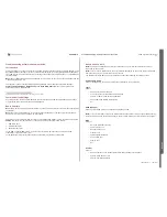
N2420 IC IF ISP1508 ES3 1200-1694
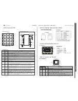
Pin Diagram
ball A1 index area
A
F
E
D
C
B
5
4
3
2
1
6
ISP1508 TFBGA36 pinout (top view)
Pin Description
Symbol
1
Ball No
Type
2
Description
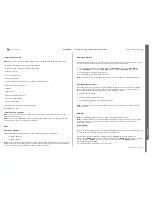
RREF
C2
AI/O
Resistor reference. Connect through 12k
: r
1% to GND.
DM
C1
AI/O
Connect to D- pin of the USB connector
x
USB mode: D- input/output
x
UART
mode:
TXD
output
DP
D1
AI/O
Connect to D+ pin of the USB connector
x
USB mode: D+ input/output
x
UART mode: RXD input
FAULT
E2
I
Input for Vbus digital over-current or fault detector signal.
If this pin is not in use, connect it to GND
Plain input, 5V tolerant
ID
D3
I
identification (ID) pin of the mini-USB cable.
If this pin is not in use, leave this pin open(there’s internal pull-up).
Plain input, TTL
VBUS
F4
AI/O
Connect to V
BUS
pin of the USB connector.
VCC
F3
P
Input supply voltage or battery source. Nominally 3.0V to 4.5V.
Note: Below 3.0V, USB FS and LS transactions are not guaranteed to
work though some devices may work with ISP1508 at these voltages.
PSW_N
D4
OD
Controls an external, active low V
BUS
power switch or charge pump.
An external pull up resistor is required.
Open drain,output, 5V tolerant.
REG3V3
E3
P
3.3V regulator output for USB mode or 2.7V regulator output for UART
mode; requiring parallel 0.1 uF and 4.7 uF capacitors. Internally
powers ATX and other analog circuits. Should not be used to power
external circuits.
XTAL1
F5
AI/O
Crystal/clock input. 1.8V peak input allowed. Frequency depends on
status on CFG1 and CFG2 pins.
XTAL2
F6
AI/O
Crystal output. If crystal is not in use, leave this pin open
CHIP_SEL
C3
I
Active HIGH chip select input.
•
When this pin is none-active, ULPI pins will be in 3-state and the chip
1
Symbol names ending with underscore N (for example, NAME_N) indicate active low signals
2
I=input; O=output; I/O = Digital Input/Output; OD = Open Drain Output; AI/O = Analog Input/Output; P = Power or
Ground pin
PIN CONNECTIONS
IN
GND
FLAG
EN
OUT
OUT
1
2
3
6
5
4
PIN FUNCTION DESCRIPTION
Pin No.
Name
Type
Description
1
EN
INPUT
Enable Pin. The device enters in shutdown mode when this pin is tied to a high level. In this case the
output is disconnected from the input. To allow normal functionality, the EN pin shall be connected to
GND to a pull down or to a I/O pin. This pin does not have an impact on the fault detection.
2
GND
POWER
Ground
3
IN
POWER
Input Voltage Pin. This pin is connected to the VBUS. A 1 F low ESR ceramic capacitor, or larger,
must be connected between this pin and GND.
4, 5
OUT
OUTPUT
Output Voltage Pin. The output is disconnected from the VBUS power supply when the input voltage is
above OVLO threshold or below UVLO threshold. A 1 F capacitor must be connected to these pins.
The two OUT pins must be hardwired to common supply.
6
FLAG
OUTPUT
Fault Indication Pin. This pin allows an external system to detect a fault on VBUS pin. The FLAG pin
goes low when input voltage exceeds OVLO threshold. Since the FLAG pin is open drain functionality,
an external pull up resistor to V
CC
must be added.
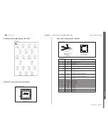
Pin-out, top view; bumps down.
N2422 ASIC Baseband 1201-4120
N2421 IC ESD Prot UDFN 6 2x2mm 1200-6309
SEMC Troubleshooting Manual
107
(124)


