C905
1222-9526 rev. 1
APPENDIX
A
P
P
E
NDIX
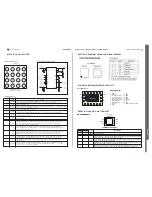
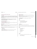
N3101 ASIC Tjatte3 CSP20 1200-9978
Pin configuration (Bump side)
1
2
3
4
5
A
B
C
D
VMIC
SPRi
SPLi
MIC
Ni
MIC
Pi
INT
mice
Gnd
INT
mici
CCO
VAD
Gnd
Gnd
Gnd
Gnd
Gnd
SPR
e
SPL
e
MIC
Ne
MIC
Pe
SPR
EF
1
2
3
4
1
5
2
3
4
5
A
B
C
D
A
B
C
D
VMIC
SPRi
SPLi
MIC
Ni
MIC
Pi
INT
mice
Gnd
INT
mici
CCO
VAD
Gnd
Gnd
Gnd
Gnd
Gnd
SPR
e
SPL
e
MIC
Ne
MIC
Pe
SPR
EF
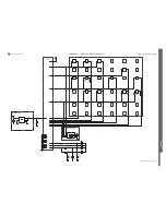
Electrical diagram
SPRi
SPLi
MICPe
GND
SPRe
SPREF
MICPi
MICNi
CCO/VMIC
VAD
MICNe
INTmici
SPLe
GND
CCO/VMIC
INTmice
R1
R7
R8
R6
R4
R5
R3
R2
SPRi
SPLi
MICPe
GND
SPRe
SPREF
MICPi
MICNi
CCO/VMIC
VAD
MICNe
INTmici
SPLe
GND
CCO/VMIC
INTmice
R1
R7
R8
R6
R4
R5
R3
R2
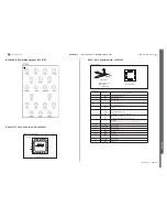
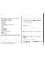
Pin configuration
(Top View, Bump Side down)
FLED
PGND
LED2
LED1
LX
MVON
SCL
LED3
FLEN
LED4
SDA
GND
OUT
IN
COMP
VDD
A1
A2
B1
C1
A3
B3
C3
B2
C2
D1
D3
D2
A4
B4
C4
D4
16-pin 2.5 x 2.5mm UCSP
3LQ 1$0(
)81&7,21
B4
IN
Analog Supply Voltage Input. The input voltage range is 2.7V to 5.5V. Bypass IN to AGND and
PGND with a 10μF ceramic capacitor as close to the IC as possible. IN is high impedance during
shutdown.
D2
GND
Analog Ground. Connect AGND to PGND
A2
PGND
Power Ground. Connect PGND toAGND and to the input capacitor ground. Also, connect PGND
to the PCB ground plane.
C4 COMP Compensation Input. Connect a
TBD
kohm resistor and
TBD
μF ceramic capacitor in series from
COMP toAGND for regulator stability.
B3
MVON
Movie On Logic Input. Connect to VDD or drive with logic 1 to enable the Movie Mode. The FLED
movie current is set in I
2
C registers. Connect toAGND or drive with logic 0 to turn off the Movie
Mode. The Movie Mode may also be enabled via the I
2
C registers.
C2
FLEN
Flash Enable Logic Input. A transition from logic 0 to logic 1 on FLEN starts the Flash Mode. The
flash duration and FLED flash current are set in I
2
C registers. The Flash Mode ends when either
FLEN transitions back to logic 0 or after the flash duration timer expires (in case FLEN gets stuck
high).
C3 SCL I
2
C Clock Input. Data is read on the rising edge of SCL.
D3 SDA I
2
C Data Input. Data is read on the rising edge of SCL.
D4
VDD
Logic Input Supply Voltage. Connect VDD to the logic supply driving SCL, SDA, MVON, and
FLEN. Bypass VDD to AGND with a 0.1μF ceramic capacitor.
B2
B1
C1
D1
LED3
LED2
LED1
LED4
LED Current Sink Regulators. Current flowing into these pins is based on the internal I
2
C
registers. Connect LED_ to the Cathodes of external LED’s. LED_ is high impedance during
shutdown. If unused, LED_ may be shorted to ground or left floating.
A1
FLED
Flash LED Current Sink Regulator. Current flowing into these pins is based on the internal I
2
C
registers. Connect FLED to the Cathode of an external Flash LED or LED Module. FLED is high
impedance during shutdown. If unused, FLED may be shorted to ground or left floating.
A4
OUT
Regulator Output. Connect OUT to the anodes of the external LED’s. Bypass OUT to PGND with
a 10μF or larger ceramic capacitor. During shutdown, OUT is one body-diode drop below the
input voltage.
A3
LX
Inductor Connection. Connect LX to the switched side of the inductor. LX is internally connected
to the drains of the internal MOSFETs. Both MOSFETs are off during shutdown.
N4400 IC Dri MAX8830 ES3 4x4 UCSP
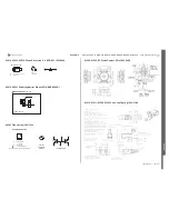
Components - N3101, N4400, S2415, V2200, V2202, V2412, V2417
5
1
6
2
3
4
MicroFET
D1
S1
G2
G1
D2
S2
PIN
D1
G2
S2
S1
G1
D2
D1
D2
PINNING
PIN
DESCRIPTION
1
cathode
2
anode
Top view
MAM387
The marking bar indicates the cathode.
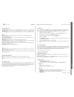
V2412, V2417 Zener Diode Voltage Regulator 15V 5% RKZ223905/2
V2202 Trans P-ch FET RYN122910/1
V2200 Zener Diode RKZ223911/1
S2415, S2424, S2453, S2454 Input Switch 1204-1127
SEMC Troubleshooting Manual
109
(124)


