SN8P2711A
8-Bit Micro-Controller
SONiX TECHNOLOGY CO., LTD
Page 7
Version 0.1
1
1
1
PRODUCT OVERVIEW
SN8P2711A
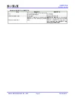
is modified from SN8P2711. Good internal high RC frequency 16MHz
±
2%. Good high
noisy protecting performance for household application.
z
SN8P2711 is compatible to SN8P2711A.
z
Better IHRC performance from 16MHz
±
5% to 16MHz
±
2%.
z
Good brown out reset production.
z
SN8P2711 code can transfer to SN8P2711A directly. Program the original SN8 of SN8P2711
into SN8P2711A directly without declare SN8P2711A in source code and re-compile again.
1.1 FEATURES
)
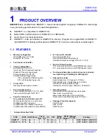
Features Selection Table
Timer
PWM
CHIP
ROM RAM Stack
TC0 TC1
I/O
ADC
Green
Mode Buzzer
Wakeup
Pin No.
Package
SN8P2711
1K*16 64
4
V
V
12 5+1 ch
V
2
5
P-DIP 14/SOP 14/SSOP 16
SN8P2711A 1K*16 64
4
V
V
12 5+1 ch
V
2
5
P-DIP 14/SOP 14/SSOP 16
♦
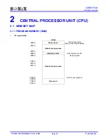
Memory configuration
♦
5+1 channel 12-bit ADC.
OTP ROM size: 1K * 16 bits.
Five external ADC input
RAM size: 64 * 8 bits.
One internal battery measurement
Internal AD reference voltage (VDD, 4V, 3V ,2V).
♦
Four levels stack buffer.
♦
Two 8-bit Timer/Counter
♦
I/O pin configuration
TC0: Auto-reload timer/Counter/PWM0/Buzzer output.
Bi-directional: P0, P4, P5.
TC1: Auto-reload timer/Counter/PWM1/Buzzer output.
Input only: P0.4 shared with reset pin.
Wakeup: P0 level change trigger.
♦
On chip watchdog timer and clock source is internal
Pull-up resisters: P0, P4, P5.
low clock RC type (16KHz @3V, 32KHz @5V).
External Interrupt trigger edge:
P0.0 controlled by PEDGE register.
♦
Dual system clocks
P0.1 is falling edge trigger only.
External high clock: RC type up to 10 MHz.
External high clock: Crystal type up to 16 MHz.
♦
3-Level LVD.
Internal high clock: 16MHz RC type.
Reset system and power monitor.
Internal low clock: RC type 16KHz(3V), 32KHz(5V).
♦
Five interrupt sources
♦
Operating modes
Three internal interrupts: TC0, TC1, ADC.
Normal mode: Both high and low clock active.
Two external interrupts: INT0, INT1.
Slow mode: Low clock only.
Sleep mode: Both high and low clock stop.
♦
Powerful instructions
Green mode: Periodical wakeup by TC0 timer
One clocks per instruction cycle (1T)
Most of instructions are one cycle only.
♦
Package (Chip form support)
All ROM area JMP instruction.
P-DIP 14 pins
All ROM area CALL address instruction.
SOP 14 pins
All ROM area lookup table function (MOVC).
SSOP 16 pins

