DX-SX1H
– 64 –
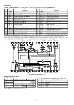
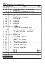
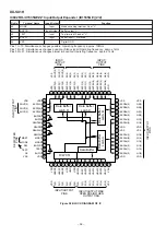
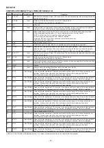
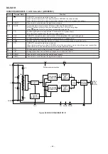
IC902 VHiADC08351-1: A/D Converter (ADC08351)
1
OE
CMOS/TTL compatible digital input terminal.
When this terminal is set to Low, digital output of ADC08351 becomes enable.
When this terminal is set to High, digital output changes to the high-impedance condition.
2
DGND
Ground return circuit terminal for digital power supply.
3-10
D0-D7
Conversion data output terminal. C0 shows LSB, and D7 shows MBS.
Effective data are output on data bus immediately after CLK input rising edge.
When OE terminal is set to Low, these terminals become enable.
11
VD
Positive digital power voltage terminal. Connected to +3V power supply.
VA and VD are supplied from the common power supply.
12
CLK
CMOS/TTL compatible clock input terminal. VIN is sampled at CLK input trailing edge.
13
VD
Positive digital power voltage terminal. Connected to +3V voltage power.
14
VREF
Positive reference voltage input terminal. Voltage of this terminal ranges from 0.75V to VA.
15
PD
CMOS/TTL compatible digital input terminal.
When this terminal is set to High, ADC08351 enters the power down mode, minimizing power consumption.
When this is set to Low, the device enters the normal operation mode.
16
VA
Positive analog power voltage terminal: To c3V voltage power.
17
VIN
Analog signal input. Convertible input ranges from 0.5Vp-p to 0.68Va.
18, 19
AGND
Ground return circuit terminal for analog power supply.
20
DGND
Ground return circuit terminal for digital power supply.
Pin No.
Terminal Name
Function
V
REF
V
IN
AGND
MUX
12k
18k
266
26
256
CLK
PD
AGND DGND
OE
DATA
OUT
(D0~D7)
8
17
17
17
8
8
8
1
99
V
D
+
V
A
+
SWITCH
ROUGH/FINE
COMPARATOR
ROUGH/FINE
COMPARATOR
Encoder and error correction
ENCODER
AND
ERROR
CORRECTION
ENCODER
AND
ERROR
CORRECTION
OUTPUT
DRIVER
CLOCK
GENERATOR
14
17
18
12
15
19
2,20
1
3
10
~
13,11
16
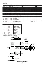
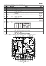
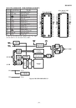
Figure 64 BLOCK DIAGRAM OF IC

