DX-SX1H
– 61 –
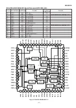
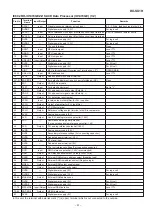
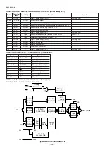
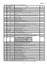
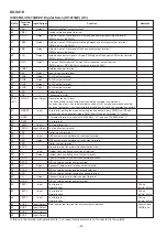
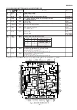
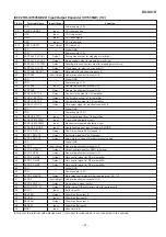
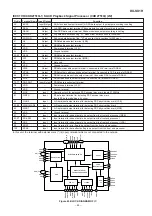
IC805 RH-iX1539GEZZ: Flash ROM (IX1539GE) (2/2)
Pin No. Terminal Name Input/Output
Function
42
DQ6
Input/Output
Lower byte data input/output: Data and command input during cycle of writing command user
interface. Memory array, identifier, and status data output when reading various data.
Float condition in case of chip non-select or output disable.
43
DQ14
Input/Output
Upper byte data input/output: The function is the same as shown in case of the lower byte data
input/output above. Operating only in x16 mode. Floating in x 8 mode. DQ15/A-1: address
44
DQ7
Input/Output
Lower byte data input/output: Data and command input during cycle of writing command user
interface. Memory array, identifier, and status data output when reading various data.
Float condition in case of chip non-select or output disable.
45
DQ15
Input/Output
Upper byte data input/output: The function is the same as shown in case of the lower byte data
input/output above. Operating only in x16 mode. Floating in x 8 mode. DQ15/A-1: address
46
GND
—
Ground
47
NC
—
Not used
48
A16
Input
Block select addresses: Select 1/32 erase block. These addresses are latched during data entry,
erase and lock block.
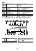
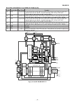
ID
REGISTOR
CSR
ESRs
DQ8-15
DQ0-7
INPUT/
OUTPUT
LOGIC
REGISTOR
BYTE#
CUI
WSM
16-KBYTE
BLOCK 31
16-KBYTE
BLOCK 30
16-KBYTE
BLOCK 1
16-KBYTE
BLOCK 0
CE#
OE#
WE#
RP#
RY/BY#
VPP
VCC
GND
Y GATE/DETECTION
Y-
DECODER
X-
DECODER
A1-17
OUTPUT
BUFFER
OUTPUT
BUFFER
INPUT
BUFFER
INPUT
BUFFER
INPUT
BUFFER
DATA QUEUE
REGISTOR
OUTPUT MULTIPLEXER
DATA
COMPARATOR
ADDRESS
QUEUE LATCH
ADDRESS COUNTER
PROGRAM
ERASE
VOLTAGE
SWITCH
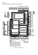
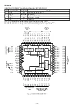
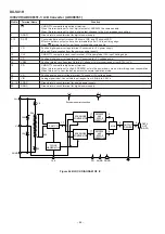
Figure 61 BLOCK DIAGRAM OF IC

