


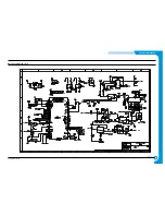

3-38
CIRCUIT DESCRIPTION
Samsung Electronics
Repair Manual
3-6 OPE PBA
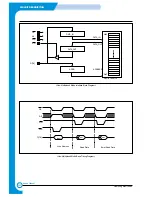
3-6-1 SUMMARY
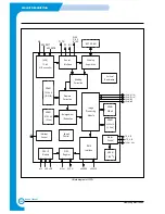
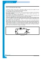
OPE Board is separated functionally from the main board and operated by the micom(Z8601) in the board. OPE and the main
use UART (universal asynchronous receiver/transmitter) channel to exchange information. OPE reset can be controlled by
the main. OPE micom controls key-scanning and LCD and LED display. If there occurs an event in OPE (such as key touch),
it sends specific codes to the main to respond to the situation and the main analyzes these codes and operates the system.
For example, it the main is to display messages in OPE, the main transmits data through UART line to OPE according to the
designated format and OPE displays this on LCD, LED. OPE’s sensing is also transmitted to the main through UART line
and then the main drives necessary operation.
OPE PBA consists of U1(MICOM, Z8601),LCD, key matrix, LED indicators. Refer to OPE Schematic Diagram and Wiring
Diagram sections of this manual.
• Signals from the key matrix are delivered to U1 input pin group (D1~D6)
• U1 pin 48 (TX DATA) is the UART code sent to MAIN PBA.
• Display from the controller is received at U1 pin 5(RX DATA).
• LCD drive signals are sent from U1 P2-x pin group, P3-4~P3-6 pins.
• Machine status LED drive signals are sent from U1 LED 1~ LED 8.
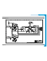
Connector
MICOM
Z8601
UART2
Reset
11
7
X
Y
8
RESONATOR
7.37 MHz
LCD
16 X 2 Line
Key Matrix
LEDs
<OPE BLOCK DIAGRAM>
Summary of Contents for SF-830
Page 112: ...Exploded Views and Parts List 5 34 Samsung Electronics ...
Page 116: ......
Page 163: ...4 2 SCHEMATIC DIAGRAMS Samsung Electronics Repair Manual Main Circuit Diagram 2 17 ...
Page 164: ...4 3 Samsung Electronics SCHEMATIC DIAGRAMS Repair Manual Main Circuit Diagram 3 17 ...
Page 165: ...4 4 SCHEMATIC DIAGRAMS Samsung Electronics Repair Manual Main Circuit Diagram 4 17 ...
Page 166: ...4 5 Samsung Electronics SCHEMATIC DIAGRAMS Repair Manual Main Circuit Diagram 5 17 ...
Page 167: ...4 6 SCHEMATIC DIAGRAMS Samsung Electronics Repair Manual Main Circuit Diagram 6 17 ...
Page 168: ...4 7 Samsung Electronics SCHEMATIC DIAGRAMS Repair Manual Main Circuit Diagram 7 17 ...
Page 169: ...4 8 SCHEMATIC DIAGRAMS Samsung Electronics Repair Manual Main Circuit Diagram 8 17 ...
Page 170: ...4 9 Samsung Electronics SCHEMATIC DIAGRAMS Repair Manual Main Circuit Diagram 9 17 ...
Page 171: ...4 10 SCHEMATIC DIAGRAMS Samsung Electronics Repair Manual Main Circuit Diagram 10 17 ...
Page 172: ...4 11 Samsung Electronics SCHEMATIC DIAGRAMS Repair Manual Main Circuit Diagram 11 17 ...
Page 173: ...4 12 SCHEMATIC DIAGRAMS Samsung Electronics Repair Manual Main Circuit Diagram 12 17 ...
Page 174: ...4 13 Samsung Electronics SCHEMATIC DIAGRAMS Repair Manual Main Circuit Diagram 13 17 ...
Page 175: ...4 14 SCHEMATIC DIAGRAMS Samsung Electronics Repair Manual Main Circuit Diagram 14 17 ...
Page 176: ...4 15 Samsung Electronics SCHEMATIC DIAGRAMS Repair Manual Main Circuit Diagram 15 17 ...
Page 177: ...4 16 SCHEMATIC DIAGRAMS Samsung Electronics Repair Manual Main Circuit Diagram 16 17 ...
Page 178: ...4 17 Samsung Electronics SCHEMATIC DIAGRAMS Repair Manual Main Circuit Diagram 17 17 ...
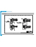
Page 180: ...4 19 Samsung Electronics SCHEMATIC DIAGRAMS Repair Manual 4 3 OPE Circuit Diagram D9 ...
Page 181: ...4 20 SCHEMATIC DIAGRAMS Samsung Electronics Repair Manual 4 4 Scan Circuit Diagram ...
Page 187: ...4 26 SCHEMATIC DIAGRAMS Samsung Electronics Repair Manual 4 8 PTL Circuit Diagram ...
Page 188: ...4 27 Samsung Electronics SCHEMATIC DIAGRAMS Repair Manual 4 10 Toner_Rx Circuit Diagram ...
Page 189: ...4 28 SCHEMATIC DIAGRAMS Samsung Electronics Repair Manual 4 11 Toner_Tx Circuit Diagram ...


