


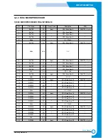

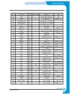
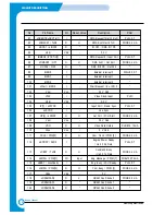
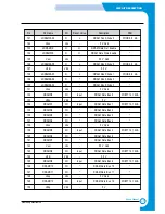
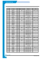

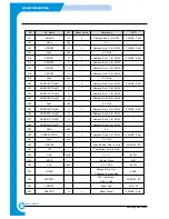


3
3-1
Samsung Electronics
CIRCUIT DESCRIPTION
Repair Manual
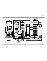
3. Circuit Description
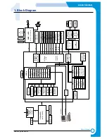
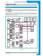
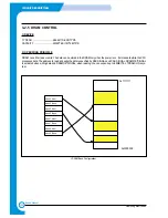
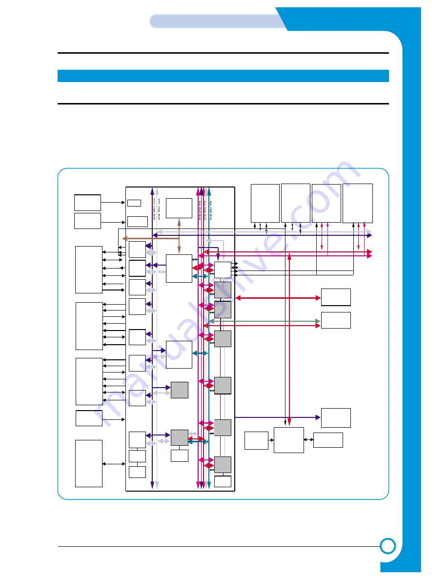
3-1 Main PBA
3-1-1 SUMMARY
The main circuit that consists of CPU, MFP controller (built-in 32bit RISC processor core: ARM7TDMI) including various I/O
device drivers, system memory, scanner, printer, motor driver, PC I/F, and FAX transceiver controls the whole system. The
entire structure of the main circuit is as follows :
OSC
20 MHz
POWER
ON RESET
MODEM
CIP3
OSC.(Video)
45.3928 MHz
LIU
OSC.
48 MHz
USB
INTERFACE IC
(UNICON)
USB
RTC
PARALLEL
INTERFACE
OPE PANEL
INTERFACE
PROGRAM
ROM
1MB x 4EA
SRAM
256K
DATA RAM
(DRAM)
8MB x 2EA
DATA RAM
(DRAM)
2MB x 2EA
PLL
Reset & WDT
Generation
ARM7TDMI
Cache 8KB
ROM/SRAM/
FLASH ROM
Control
(4 Bank)
I/O
Control
(5 Bank)
CPU BUS
Interface Block
GPIO
SYSTEM BUS
Interface Block
[Arbiter]
VIS
ADC
RAM : 512B
UART
(3 CH)
Interrupt
Control
(4 External)
Timer
(3 CH)
Tone
Generator
Engine
Comm. I/F
JBIG
LRAM:1296B
CXRAM:256B
RAM
512B+512B
HPVC
PPI
PVC
GEU
EDO/FPM
DRAM
Control
(4 Bank)
MA
MD
RAS
CAS
/CS,/RD,/WR
A/D BUS
IOCS
PM-22
DMAC
(2 CH)
HCT
IMCS
/MIR0,
/RD,/WR
D0~D7
A0~A4
RST_OUT
/RST_OUT
/XDACK
/XDREQ
/SDIP CS
/RD,/WR
D0~D15
A0~A5
ID01 ~ ID15
OD0 ~ OD15
RA0 ~ RA15
/CS
CLOCK
/RD
NOR
• Main B’D
<Block Diagram>
Summary of Contents for SF-830
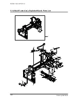
Page 112: ...Exploded Views and Parts List 5 34 Samsung Electronics ...
Page 116: ......
Page 163: ...4 2 SCHEMATIC DIAGRAMS Samsung Electronics Repair Manual Main Circuit Diagram 2 17 ...
Page 164: ...4 3 Samsung Electronics SCHEMATIC DIAGRAMS Repair Manual Main Circuit Diagram 3 17 ...
Page 165: ...4 4 SCHEMATIC DIAGRAMS Samsung Electronics Repair Manual Main Circuit Diagram 4 17 ...
Page 166: ...4 5 Samsung Electronics SCHEMATIC DIAGRAMS Repair Manual Main Circuit Diagram 5 17 ...
Page 167: ...4 6 SCHEMATIC DIAGRAMS Samsung Electronics Repair Manual Main Circuit Diagram 6 17 ...
Page 168: ...4 7 Samsung Electronics SCHEMATIC DIAGRAMS Repair Manual Main Circuit Diagram 7 17 ...
Page 169: ...4 8 SCHEMATIC DIAGRAMS Samsung Electronics Repair Manual Main Circuit Diagram 8 17 ...
Page 170: ...4 9 Samsung Electronics SCHEMATIC DIAGRAMS Repair Manual Main Circuit Diagram 9 17 ...
Page 171: ...4 10 SCHEMATIC DIAGRAMS Samsung Electronics Repair Manual Main Circuit Diagram 10 17 ...
Page 172: ...4 11 Samsung Electronics SCHEMATIC DIAGRAMS Repair Manual Main Circuit Diagram 11 17 ...
Page 173: ...4 12 SCHEMATIC DIAGRAMS Samsung Electronics Repair Manual Main Circuit Diagram 12 17 ...
Page 174: ...4 13 Samsung Electronics SCHEMATIC DIAGRAMS Repair Manual Main Circuit Diagram 13 17 ...
Page 175: ...4 14 SCHEMATIC DIAGRAMS Samsung Electronics Repair Manual Main Circuit Diagram 14 17 ...
Page 176: ...4 15 Samsung Electronics SCHEMATIC DIAGRAMS Repair Manual Main Circuit Diagram 15 17 ...
Page 177: ...4 16 SCHEMATIC DIAGRAMS Samsung Electronics Repair Manual Main Circuit Diagram 16 17 ...
Page 178: ...4 17 Samsung Electronics SCHEMATIC DIAGRAMS Repair Manual Main Circuit Diagram 17 17 ...
Page 180: ...4 19 Samsung Electronics SCHEMATIC DIAGRAMS Repair Manual 4 3 OPE Circuit Diagram D9 ...
Page 181: ...4 20 SCHEMATIC DIAGRAMS Samsung Electronics Repair Manual 4 4 Scan Circuit Diagram ...
Page 187: ...4 26 SCHEMATIC DIAGRAMS Samsung Electronics Repair Manual 4 8 PTL Circuit Diagram ...
Page 188: ...4 27 Samsung Electronics SCHEMATIC DIAGRAMS Repair Manual 4 10 Toner_Rx Circuit Diagram ...
Page 189: ...4 28 SCHEMATIC DIAGRAMS Samsung Electronics Repair Manual 4 11 Toner_Tx Circuit Diagram ...


