3-24
CIRCUIT DESCRIPTION
Samsung Electronics
Repair Manual
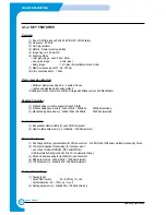
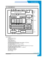
3-3-2 KEY FEATURES
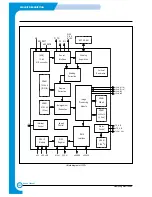
Overview
(1) 0.5µm C-MOS process(TLM), 208-PIN QFP, STD85 library
(2) Frequency : 50 MHz
(3) On-Chip oscillator
(4) Method : Raster scanning method
(5) Image Sauce : 300 dpi CIS
(6) Scanning Mode
• color gray image : each 8 bits / RGB
• mono gray image
: 8 bits / pixel
• binary image
: 1 bit / pixel (for text/photo/mixed mode)
(7) Maximum scanning width : A4, 300 dpi
(8) A/D conversion depth : 12bits
Pixel processing structure
• Minimum pixel processing time : 4 system clocks
• High speed pipelined processing method
(Shading correction, Gamma correction, Enlargement/Reducement, and Binarization)
Shading Correction
(1) White shading correction support for each R/G/B
(2) White shading data memory : 3x8Kx12bits = 288Kbits 384Kbits (external)
(3) Black shading data memory : 3x8Kx12bits = 288Kbits 384Kbits (external)
Gamma Correction
(1) Independent Gamma table for each RGB component
(2) Gamma table data memory : 3x1Kx8bits = 24Kbits (internal)
Binarization (mono)
(1) 256 Gray’s halftone representation for Photo document : 3x5 EDF(Error DifFusion) method proposed by Stuck.
(2) LAT(Local Adaptive Thresholding) for Text document :
• use of 5x5 LOCAL WINDOW (TIP ALGORITHM)
• ABC(Automatic Background Control) :Tmin Automatic change
(3) Mixed mode processing for text/photo mixed document
(4) EDF data memory : 2x4Kx16bits = 128Kbits (internal)
(5) LAT data memory : 4x4Kx16bits = 256Kbits (external)
Scaling of input image
(1) Scaling factor
• Horizontal direction
: 25 ~ 800% by 1% unit
• Vertical direction : 25 ~ 100% by 1% unit
(2) Scaling data memory : 2x8Kx8bits = 128Kbits (internal)
Summary of Contents for SF-830
Page 112: ...Exploded Views and Parts List 5 34 Samsung Electronics ...
Page 116: ......
Page 163: ...4 2 SCHEMATIC DIAGRAMS Samsung Electronics Repair Manual Main Circuit Diagram 2 17 ...
Page 164: ...4 3 Samsung Electronics SCHEMATIC DIAGRAMS Repair Manual Main Circuit Diagram 3 17 ...
Page 165: ...4 4 SCHEMATIC DIAGRAMS Samsung Electronics Repair Manual Main Circuit Diagram 4 17 ...
Page 166: ...4 5 Samsung Electronics SCHEMATIC DIAGRAMS Repair Manual Main Circuit Diagram 5 17 ...
Page 167: ...4 6 SCHEMATIC DIAGRAMS Samsung Electronics Repair Manual Main Circuit Diagram 6 17 ...
Page 168: ...4 7 Samsung Electronics SCHEMATIC DIAGRAMS Repair Manual Main Circuit Diagram 7 17 ...
Page 169: ...4 8 SCHEMATIC DIAGRAMS Samsung Electronics Repair Manual Main Circuit Diagram 8 17 ...
Page 170: ...4 9 Samsung Electronics SCHEMATIC DIAGRAMS Repair Manual Main Circuit Diagram 9 17 ...
Page 171: ...4 10 SCHEMATIC DIAGRAMS Samsung Electronics Repair Manual Main Circuit Diagram 10 17 ...
Page 172: ...4 11 Samsung Electronics SCHEMATIC DIAGRAMS Repair Manual Main Circuit Diagram 11 17 ...
Page 173: ...4 12 SCHEMATIC DIAGRAMS Samsung Electronics Repair Manual Main Circuit Diagram 12 17 ...
Page 174: ...4 13 Samsung Electronics SCHEMATIC DIAGRAMS Repair Manual Main Circuit Diagram 13 17 ...
Page 175: ...4 14 SCHEMATIC DIAGRAMS Samsung Electronics Repair Manual Main Circuit Diagram 14 17 ...
Page 176: ...4 15 Samsung Electronics SCHEMATIC DIAGRAMS Repair Manual Main Circuit Diagram 15 17 ...
Page 177: ...4 16 SCHEMATIC DIAGRAMS Samsung Electronics Repair Manual Main Circuit Diagram 16 17 ...
Page 178: ...4 17 Samsung Electronics SCHEMATIC DIAGRAMS Repair Manual Main Circuit Diagram 17 17 ...
Page 180: ...4 19 Samsung Electronics SCHEMATIC DIAGRAMS Repair Manual 4 3 OPE Circuit Diagram D9 ...
Page 181: ...4 20 SCHEMATIC DIAGRAMS Samsung Electronics Repair Manual 4 4 Scan Circuit Diagram ...
Page 187: ...4 26 SCHEMATIC DIAGRAMS Samsung Electronics Repair Manual 4 8 PTL Circuit Diagram ...
Page 188: ...4 27 Samsung Electronics SCHEMATIC DIAGRAMS Repair Manual 4 10 Toner_Rx Circuit Diagram ...
Page 189: ...4 28 SCHEMATIC DIAGRAMS Samsung Electronics Repair Manual 4 11 Toner_Tx Circuit Diagram ...

