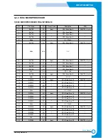

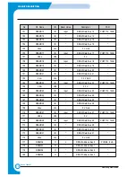

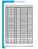


3-17
Samsung Electronics
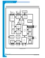
CIRCUIT DESCRIPTION
Repair Manual
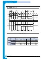
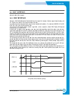
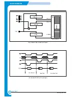
3-2-6 FS781 (FREQUENCY ATTENUATOR)
This system used FS781 for the main clock for EMI SUPPRESSION.
It spreads the source clock in a consistent bandwidth to disperse the energy gathered in order to attenuate the energy.
The capacitor value of the loop filter(PIN 4) is set depending on the source clock used or the spread bandwidth. Refer to
FS781 Spec. for detail.
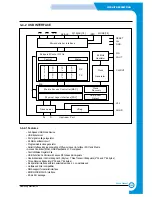
3-2-7 USB (UNIVERSAL SERIAL BUS)
NS’s USBN9602 is used as the interface IC and 48MHz clock is used.
When the data is received through the USB port, EIRQ1 SIGNAL is activated to send interrupt to CPU, then it directly sends
the data to DRAM by IOCS4*&DRAMA(11) SIGNAL through DRAMD (24;31).
3-2-8 SRAM; 32KB SRAM
It stores a variety of option data.
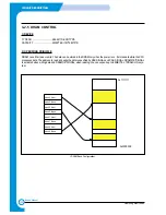
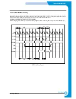
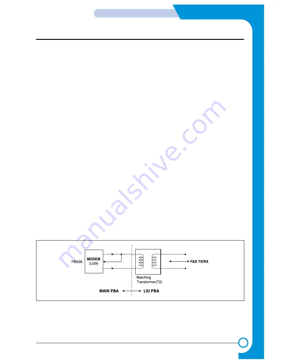
3-2-9 FAX TRANSCEIVER (Only SCX-5312F)
3-2-9-1. GENERAL
This circuit processes transmission signals of modem and between LIU and modem.
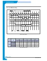
3-2-9-2. MODEM (U39)
FM336 is a single ship fax modem. It has functions of DTMF detection and DTMF signal production as well as functions of
modem. TX A1, 2 is transmission output port and RX IN is received data input port. / POR signal controlled by MFP controller
(U36:KS32C61200) can initialize modem (nMODEM_RST) without turning off the system.
D0-D7 are 8-bit data buses. RS0-RS4 signals to select the register in modem chips. /RS and /WR signals control READ and
WRITE respectively. /IRQ is a signal for modem interrupt.
Transmission speed of FM336 is supported up to 33.6k. The modem is connected to LINE through transformer directly.
< FAX TRANSCEIVER >
Summary of Contents for SF-830
Page 112: ...Exploded Views and Parts List 5 34 Samsung Electronics ...
Page 116: ......
Page 163: ...4 2 SCHEMATIC DIAGRAMS Samsung Electronics Repair Manual Main Circuit Diagram 2 17 ...
Page 164: ...4 3 Samsung Electronics SCHEMATIC DIAGRAMS Repair Manual Main Circuit Diagram 3 17 ...
Page 165: ...4 4 SCHEMATIC DIAGRAMS Samsung Electronics Repair Manual Main Circuit Diagram 4 17 ...
Page 166: ...4 5 Samsung Electronics SCHEMATIC DIAGRAMS Repair Manual Main Circuit Diagram 5 17 ...
Page 167: ...4 6 SCHEMATIC DIAGRAMS Samsung Electronics Repair Manual Main Circuit Diagram 6 17 ...
Page 168: ...4 7 Samsung Electronics SCHEMATIC DIAGRAMS Repair Manual Main Circuit Diagram 7 17 ...
Page 169: ...4 8 SCHEMATIC DIAGRAMS Samsung Electronics Repair Manual Main Circuit Diagram 8 17 ...
Page 170: ...4 9 Samsung Electronics SCHEMATIC DIAGRAMS Repair Manual Main Circuit Diagram 9 17 ...
Page 171: ...4 10 SCHEMATIC DIAGRAMS Samsung Electronics Repair Manual Main Circuit Diagram 10 17 ...
Page 172: ...4 11 Samsung Electronics SCHEMATIC DIAGRAMS Repair Manual Main Circuit Diagram 11 17 ...
Page 173: ...4 12 SCHEMATIC DIAGRAMS Samsung Electronics Repair Manual Main Circuit Diagram 12 17 ...
Page 174: ...4 13 Samsung Electronics SCHEMATIC DIAGRAMS Repair Manual Main Circuit Diagram 13 17 ...
Page 175: ...4 14 SCHEMATIC DIAGRAMS Samsung Electronics Repair Manual Main Circuit Diagram 14 17 ...
Page 176: ...4 15 Samsung Electronics SCHEMATIC DIAGRAMS Repair Manual Main Circuit Diagram 15 17 ...
Page 177: ...4 16 SCHEMATIC DIAGRAMS Samsung Electronics Repair Manual Main Circuit Diagram 16 17 ...
Page 178: ...4 17 Samsung Electronics SCHEMATIC DIAGRAMS Repair Manual Main Circuit Diagram 17 17 ...
Page 180: ...4 19 Samsung Electronics SCHEMATIC DIAGRAMS Repair Manual 4 3 OPE Circuit Diagram D9 ...
Page 181: ...4 20 SCHEMATIC DIAGRAMS Samsung Electronics Repair Manual 4 4 Scan Circuit Diagram ...
Page 187: ...4 26 SCHEMATIC DIAGRAMS Samsung Electronics Repair Manual 4 8 PTL Circuit Diagram ...
Page 188: ...4 27 Samsung Electronics SCHEMATIC DIAGRAMS Repair Manual 4 10 Toner_Rx Circuit Diagram ...
Page 189: ...4 28 SCHEMATIC DIAGRAMS Samsung Electronics Repair Manual 4 11 Toner_Tx Circuit Diagram ...


