3-36
CIRCUIT DESCRIPTION
Samsung Electronics
Repair Manual
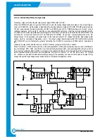
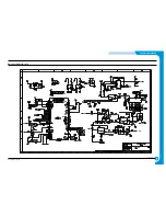
3-5-7-6. THV(THV(+)/THV(-) Output Unit)
Tr) output unit is the transfer output control signal 'PWM-LOW ACTIVE'.
When THV-PWM LOW signal is received, Q203 turns on and the steady voltage will be accepted to the non-inverting ter-
minal of OP-AMP 324. As the voltage is higher than the inverting reference voltage of OP-AMP, OP-AMP output turns high.
The 24V power adjusts the electric potential to ZD201 and ZD202, sends IB to TRANS auxiliary wire through current-
restricting resistance R215 via R212 and C204, and eventually Q204 will turn on. When the current is accepted to Q402,
Ic increases to the current proportional to time through the T201 primary coil, and when it reaches the Hfe limit of Q204, it will
not retain the "on" state, but will turn to "off". As Q402 turns 'off', TRANS N1 will have counter-electromotive force, dis-
charge energy to the secondary coil, sends current to the load and outputs THV voltage through the high voltage output
enable, which is comprised of Regulation– circuit. The output voltage is determined by the DUTY width. Q203 switches
with PWM DUTY cycle to fluctuate the output by fluctuating the OP-AMP non-inverting end VREF electric potential, and
the
maximum is output at 0% and the minimum, at 100%.Transfer(-) output unit is THV-EA 'L' enable.
When THV-EA is 'L', Q302 turns on and the VCE electric potential of Q302 will be formed and sends IB to TRANS auxil-
iary wire through R311, C305 and VR302 via current-restricting resistance R314, and eventually Q303 will turn on. When
the current is accepted to Q303, Q303's Ic increases to the current proportional to time through the T301 primary coil, and
when it reaches the Hfe limit of Q303, it will not retain the "on" state, but will turn to "off". As Q303 turns 'off', TRANS
N1 will have counter-electromotive force, discharge energy to the secondary coil, send current to load and output THV(-)
voltage through the high voltage output enable, which is comprised of Regulation– circuit.
#7
TEV-PWM
5V
U2
1
2
3
R201
10K
U2
R205
1.8K
R206
100
Q203
A708Y
R208
30K
18V
R209
100KF
VR201
50K
R207
2K
C201
103
C202
121
R210
845KF
D202
1N4148
R211
1MF
5
6
7
+
_
U1
11 KA324
24VS
+
C101
35V47
U
F
D201
1N4148
24VS
R213
2.2K
R212
680K
C203
472
D203
1N4148
ZD201
5.65V
ZD202
705V
R214
2.2K
C204
333Z
Q204
D526
T201
KAB-007
C206
6KV470pF
C205
2KV68pF
D204
6KV
D206
6KV
C209
6KV
C208
6KV
D205
6KV
D207
6KV
R215
390
C207
3KV470pF
R216
SBR306
R218
MGR1/2W100KF
R217
SBR207
#17
#19
#5
#24
5V
TEV-EA
TEV-READ
5V
D301
1N4148
5
6
7
U2
7407
D-GND
24VS
C4
103
8
9
10
U1
+
_
KA324
R301
470K
C301
222
R302
33K
R303
100KF
C302
102
D302
1N4148
C303
103
R304
389KF
R305
10KF
VR301
5K
R306
26.1KF
C304
500V103Z
18V
R309
202K
R307
33K
Q301
A708Y
18V
R310
2.2K
R308
33K
Q302
A708Y
R312
1W56
R313
1W56
Q303
D526
R311
100KF
C305
333Z
VR302
2K
R314
1.7K
KAB-006
T301
1
5
2
4
6
7
1
5
2
4
7
6
C307
3KW470pF
D304
4KV
C306
2KV68pF
D303
4KV
C308
3KV470pF
R315
SBR306
Summary of Contents for SF-830
Page 112: ...Exploded Views and Parts List 5 34 Samsung Electronics ...
Page 116: ......
Page 163: ...4 2 SCHEMATIC DIAGRAMS Samsung Electronics Repair Manual Main Circuit Diagram 2 17 ...
Page 164: ...4 3 Samsung Electronics SCHEMATIC DIAGRAMS Repair Manual Main Circuit Diagram 3 17 ...
Page 165: ...4 4 SCHEMATIC DIAGRAMS Samsung Electronics Repair Manual Main Circuit Diagram 4 17 ...
Page 166: ...4 5 Samsung Electronics SCHEMATIC DIAGRAMS Repair Manual Main Circuit Diagram 5 17 ...
Page 167: ...4 6 SCHEMATIC DIAGRAMS Samsung Electronics Repair Manual Main Circuit Diagram 6 17 ...
Page 168: ...4 7 Samsung Electronics SCHEMATIC DIAGRAMS Repair Manual Main Circuit Diagram 7 17 ...
Page 169: ...4 8 SCHEMATIC DIAGRAMS Samsung Electronics Repair Manual Main Circuit Diagram 8 17 ...
Page 170: ...4 9 Samsung Electronics SCHEMATIC DIAGRAMS Repair Manual Main Circuit Diagram 9 17 ...
Page 171: ...4 10 SCHEMATIC DIAGRAMS Samsung Electronics Repair Manual Main Circuit Diagram 10 17 ...
Page 172: ...4 11 Samsung Electronics SCHEMATIC DIAGRAMS Repair Manual Main Circuit Diagram 11 17 ...
Page 173: ...4 12 SCHEMATIC DIAGRAMS Samsung Electronics Repair Manual Main Circuit Diagram 12 17 ...
Page 174: ...4 13 Samsung Electronics SCHEMATIC DIAGRAMS Repair Manual Main Circuit Diagram 13 17 ...
Page 175: ...4 14 SCHEMATIC DIAGRAMS Samsung Electronics Repair Manual Main Circuit Diagram 14 17 ...
Page 176: ...4 15 Samsung Electronics SCHEMATIC DIAGRAMS Repair Manual Main Circuit Diagram 15 17 ...
Page 177: ...4 16 SCHEMATIC DIAGRAMS Samsung Electronics Repair Manual Main Circuit Diagram 16 17 ...
Page 178: ...4 17 Samsung Electronics SCHEMATIC DIAGRAMS Repair Manual Main Circuit Diagram 17 17 ...
Page 180: ...4 19 Samsung Electronics SCHEMATIC DIAGRAMS Repair Manual 4 3 OPE Circuit Diagram D9 ...
Page 181: ...4 20 SCHEMATIC DIAGRAMS Samsung Electronics Repair Manual 4 4 Scan Circuit Diagram ...
Page 187: ...4 26 SCHEMATIC DIAGRAMS Samsung Electronics Repair Manual 4 8 PTL Circuit Diagram ...
Page 188: ...4 27 Samsung Electronics SCHEMATIC DIAGRAMS Repair Manual 4 10 Toner_Rx Circuit Diagram ...
Page 189: ...4 28 SCHEMATIC DIAGRAMS Samsung Electronics Repair Manual 4 11 Toner_Tx Circuit Diagram ...


