background image

ELECTRONICS

©

Samsung Electronics Co., Ltd. 

JULY. 2002

Printed in Korea

AA82-00093A

Summary of Contents for CFTD2083TX/SMS

Page 1: ...S DVD Television Cassette Recorder CONTENTS Precautions Specifications Disassembly and Reassembly Alignment and Adjustment Electrical Troubleshooting Exploded View and Parts List Electric Parts List Block Diagram Schematic Diagrams 1 2 3 4 5 6 7 8 9 ...

Page 2: ...ELECTRONICS Samsung Electronics Co Ltd JULY 2002 Printed in Korea AA82 00093A ...

Page 3: ...ts metal cabinets screwheads and control shafts The current measured should not exceed 0 5 milliamp Reverse the power plug prongs in the AC outlet and repeat the test Fig 1 1 AC Leakage Test 6 Antenna Cold Check With the unit s AC plug disconnected from the AC source connect an electrical jumper across the two AC prongs Connect one lead of the ohmmeter to an AC prong Connect the other lead to the ...

Page 4: ...t appear to have overheated or that are otherwise damaged should be replaced with parts that meet the original specifications Always determine the cause of damage or overheat ing and correct any potential hazards 15 Observe the original lead dress especially near the following areas Antenna wiring sharp edges and especially the AC and high voltage power supplies Always inspect for pinched out of p...

Page 5: ...ssible conductive parts examples metal panels input terminals and earphone jacks 6 Insulation Checking Procedure Disconnect the power cord from the AC source and turn the power switch ON Connect an insulation resistance meter 500V to the blades of the AC plug The insulation resistance between each blade of the AC plug and accessible conductive parts see above should be greater than 1 megohm 7 Neve...

Page 6: ...n anti static solder removal device Many solder removal devices are not rated as anti static these can accumulate sufficient electrical charge to damage ESDs 7 Do not remove a replacement ESD from its protective package until you are ready to install it Most replacement ESDs are packaged with leads that are electrically shorted together by conductive foam aluminum foil or other conductive material...

Page 7: ...e sheet This gives them the same ground as the sheet 4 Remove the optical pick up block 5 Perform work on top of the conductive sheet Be careful not to let your clothes or any other static sources to touch the unit Be sure to put on a wrist strap grounded to the sheet Be sure to lay a conductive sheet made of copper etc Which is grounded to the table Fig 1 2 6 Short the short terminal on the PCB w...

Page 8: ... Assy 3 Make solder land 2 points short on Pich up See Fig 1 3 4 Disassembly the Pick up 1 5 2 Assembly 1 Replace the Pick up 2 Remove the soldering 2 points on Pick up 3 Reassemble the Deck Assy SOLDER LAND 2 POINTS SHORT PICK UP ASS Y Note If the assembly and disassembly are not done in correct sequence the Pick up may be damaged Fig 1 3 ...

Page 9: ...Samsung Electronics 3 1 2 Specifications ...

Page 10: ...MEMO 3 2 Samsung Electronics ...

Page 11: ...Disassembly and Reassembly Samsung Electronics 3 1 1 Remove the screws located on the side of the back cover 3 Disassembly and Reassembly 3 1 Disassembly 3 1 1 Back Cover Removal ...

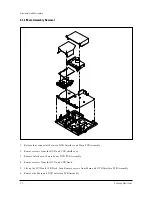
Page 12: ...D Interface and Main PCB Assembly 2 Remove screws from the DVD and VCR shield case 3 Remove shield case then take out DVD PCB Assembly 4 Remove screws from the DVD and VCR Deck 5 Life up the DVD and VCR Deck then Remove screws from Main and DVD Interface PCB Assembly 6 Remove the Main and DVD Interface PCB Assembly ...

Page 13: ...Disassembly and Reassembly Samsung Electronics 3 3 3 1 3 Power Assembly Removal 1 Release two connectors between Power and Main PCB Assembly 2 Remove screws from the Power Assembly ...

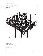
Page 14: ...mbly 3 4 Samsung Electronics Œ ˇ ˆ Ø Fig 3 1 Top parts Location 1 Œ GEAR FL CAM MOTOR LOADING ASS Y ˇ LEVER FL ARM ASS Y HOLDER FL CASSETTE ASS Y ˆ LEVER FL DOOR Ø SLIDER FL DRIVE 3 2 VCR Deck Parts Locations 3 2 1 Top View ...

Page 15: ... ˇ ˆ Ø Ô Ò Fig 3 2 Top Parts Location 2 Œ FE HEAD CYLINDER ASS Y ˇ ACE HEAD ASS Y LEVER UNIT PINCH ASS Y ˆ LEVER 9 GUIDE ASS Y Ø LEVER TENSION ASS Y BAND BRAKE ASS Y DISK S REEL LEVER S BRAKE ASS Y GEAR IDLE Ô LEVER IDLE LEVER T BRAKE ASS Y Ò DISK T REEL ...

Page 16: ...ung Electronics 3 2 2Bottom View Œ ˇ ˆ Ø Fig 3 3 Bottom Parts Location Œ GEAR JOINT 1 GEAR JOINT 2 ˇ BRACKET GEAR MOTOR CAPSTAN ASS Y ˆ LEVER T LOAD ASS Y Ø GEAR LOADING DRIVE LEVER S LOAD ASS Y HOLDER CLUTCH ASS Y BELT PULLEY SLIDER CAM ...

Page 17: ...y Œ as grasp ing the Holder FL Cassette Ass y Œ and Lever FL Cassette R in the same time to release hooking from Main Base until the Boss A of Holder FL Cassette Ass y Œ is taken out from the Rail B 3 Lift the Holder FL Cassette Ass y Œ in this time you have to grasp the Lever FL Cassette R Continuously until the Holder FL Cassette Ass y Œ is taken out completely Note Be sure to insert Lever FL Ca...

Page 18: ... 3 Slider FL Drive Gear FL Cam Removal 1 Pull the Slider FL Drive Œ to the front direc tion 2 Remove the Slider FL Drive Œ in the direction of arrow Refer to Fig 3 6 3 Remove the Gear FL cam Note When reinstalling be sure to reassemble Slider FL drive Œ after you insert the Boss of Lever FL ARM R in Groove of Slider Fl drive Œ Assembly Align the Gear FL Cam Œ with the Gear worm wheel Post as shown...

Page 19: ... Gear Worm Wheel Removal 1 Remove the Gear Worm wheel Œ Œ GEAR WORM WHEEL Fig 3 9 Gear Worm Wheel Removal 3 3 6 Motor Loading Ass y Removal 1 Remove the screw Œ 2 Remove the Motor Loading Ass y MOTOR LOADING ASS Y Œ SCREW Fig 3 10 Motor Loading Ass y Removal ...

Page 20: ... GEAR JOINT 2 3 3 8 Gear Loading Drive Slider Cam Lever Load S T Ass y Removal 1 Remove the Belt Pulley Refer to Fig 3 30 2 Remove the Gear Loading Drive Œ after releas ing Hook A in the direction arrow as shown in detail drawing 3 Remove the Slider Cam 4 Remove the Lever Load ˇ Link Load ˆ Lever Load Link Load Ø Œ GEAR LOADING DRIVE ˆ LINK LOAD S ˇ LEVER LOAD S LEVER LOAD T Ø LINK LOAD T SLIDE CA...

Page 21: ...ot of Gear Loading Drive Refer to Timing Point 2 4 Aline dot of Gear Loading drive with mark of Slider Cam ˇ as shown in drawing Refer to Timing Point 3 LEVER LOAD S Œ LEVER LOAD T LEVER LOAD S LEVER LOAD T PIN A PIN C PIN B PIN D ˇ SLIDER CAM TIMING POINT 2 TIMING POINT 1 TIMING POINT 3 3 3 10 Lever Pinch Drive Lever Tension Drive Removal 1 Remove the Lever Pinch Drive Œ Lever Tension Drive Œ LEV...

Page 22: ...n Ass y seated Rotate stop per of Main Base to the Mark B Œ SPRING TENTION LEVER STOPPER MARK B A LEVER TENTION ASS Y ˇ BAND BRAKE ASS Y 3 3 12 Lever Brake S T Ass y Removal 1 Release the Hook A and the Hook B C in the direction of arrow as shown in Fig 3 17 2 Lift the Lever S T Brake Ass y Œ with spring brake ˇ Assembly 1 Assembly the Lever S Brake Ass y Œ on the Main Base 2 Assembly the Lever T ...

Page 23: ...in the direction of arrow A B 2 Lift the Lever Idle Œ Assembly 1 Apply oil in two Bosses of Lever Idle Œ 2 Assemble the Gear Idle with the Lever Idle Œ Note When replacing the Gear Idle be sure to add oil in the boss of Lever Idle Œ 3 3 14 Disk S T Reel Removal 1 Lift the Disk S T Reel Œ GEAR IDLE GEAR IDLE Œ LEVER IDLE A HOOK C B Fig 3 18 Gear Idle Ass y Removal ...

Page 24: ...ion of arrow as shown Fig 3 21 and lift the Lever Up Down Ass y Œ 2 Lift the Gear Center Ass y Assembly 1 Insert the Lever Up Down Ass y Œ in the rec tangular holes on Main Base as shown in Fig 3 22 2 Lift the Lever Up Down Ass y Œ about 35 Refer to Fig 3 22 3 Insert Ring of the Gear Center Ass y in the Guide of the Lever Up Down Ass y Œ 4 Insert the Gear Center Ass y in the post on Main Base 5 Pu...

Page 25: ...e extreme care not to touch the grease on the Roller Pinch 2 When reinstalling be sure to apply grease on the post pinch roller ˇ SPRING PINCH DRIVE Œ LEVER UNIT PINCH ASS Y PLATE JOINT Fig 3 23 Guide Cassette Door Removal Fig 3 24 Lever Unit Pinch Ass y Plate Joint Spring Pinch Drive Removal 3 3 17 Guide Cassette Door Removal 1 Lift the Hook A 2 Rotate the Guide Cassette Door Œ in the direc tion ...

Page 26: ... direc tion of arrow A Note 1 Take extreme care not to get grease on the tape Guide Post 2 After reinstalling check the bottom side of the Post 9 Guide to the top side of Main Base Œ SPRING 9 GUIDE LEVER 9 GUIDE ASS Y A B Fig 3 25 Lever 9 Guide Ass y Removal 3 3 20 FE Head Removal 1 Remove the screw Œ 2 Lift the FE Head Œ FE HEAD Fig 3 26 FE Head Removal ...

Page 27: ...connector of ACE Head Ass y 2 Remove the screw Œ 3 Lift the ACE Head Ass y Œ SCREW HEAD ACE ASS Y 3 3 22 Slider S T Ass y Removal 1 Move the Slider S T Ass y Œ to slot and then lift it to remove Refer to arrow Œ SLIDER S ASS Y SLIDER T ASS Y Fig 3 27 ACE Head Removal Fig 3 28 Slider S T Ass y Removal ...

Page 28: ...s Œ Note 1 Take care not to touch the Cylinder Ass y ˇ and the tape guide post at reinstalling 2 When reinstalling Don t push down too much on Screw Driver Œ 3 SCREWS PLATE GROUND DECK ˇ CYLINDER ASS Y Fig 3 29 Plate Ground Deck Cylinder Ass y Removal 3 3 24 Belt Pulley Removal 1 Remove the Belt Pulley Œ Note Take extreme care not to get grease on Belt Pulley Œ at assembling or reassembling Œ BELT...

Page 29: ...ˇ MOTOR CAPSTAN ASS Y 3 3 27 How to Eject the Cassette Tape If the unit does not operate on condition that is inserted into housing ass y 1 Turn the Gear worm Œ clockwise with screw driver Refer to arrow Other method Remove the Screw of Motor Load Ass y Separate the Motor Load Ass y Œ GEAR WORM Fig 3 32 Damper Capstan Motor Capstan Ass y Removal Fig 3 33 How to Eject the Cassette Tape 2 When Slide...

Page 30: ... HEAD CYLINDER ASS Y PINCH ROLLER GUIDE ROLLER S GUIDE ROLLER T 8 GUIDE POST 9 GUIDE POST CAPSTAN SHAFT ACE HEAD 3 GUIDE POST 3 4 Tape Transport System and Adjustment Locations The tape transport system has been adjusted precisely in the factory Alignment is not necessary except for the following 1 Noise observed on the screen 2 Tape damage 3 Parts replacement in the tape transport system Lower fl...

Page 31: ...y turn the screw A tilt adjust on the ACE head ass y 4 Reconfirm the ACE head height Fig 3 5 3 Tape Guide Check 3 5 1 c AUDIO AZIMUTH ADJUSTMENT 1 Load alignment tape Mono scope and play back the NTSC 7KHz PAL 6KHz signal 2 Connect channel 1 scope probe to audio output Monitor Output 3 Adjust screw B to achieve maximum audio level See Fig 3 5 1 4 5 1 d ACE HEAD POSITION X POINT ADJUSTMENT 1 See Al...

Page 32: ...djusting driver into the X position adjusting gear and adjust the driver for maximum envelope waveform Note Do not adjust the X point using excessive force After turning the X point adjusting screw D counteerclock wise a little perform the adjustment and then tighten the screw See Fig 3 5 1 7 msec CH 2 PROBE H D SW PULSE CH 1 PROBE CTL PULSE Time div 5 msec Setting of Scope Volt div CH 1 0 1V CH 2...

Page 33: ...the video RF envelope at the exit side 4 If the section A in Fig 3 5 5 does not meet the speci fication adjust the guide roller S up or down 5 If the section B in Fig 3 5 5 does not meet the speci fication adjust the guide roller T up or down Fig 3 5 4 Envelope Waveform Adjustment a a b c d c b d a 63 b c d Fig 3 5 5 Adjustment Points A B A B H D SWITCHING PULSE ENVELOPE 6 Play back the Mono Scope...

Page 34: ...n the unit using with T 120 E 120 The video envelope should meet the specifica tion as shown in Fig 3 5 8 In SP mode A should equal B If the head gap is wide upper cylinder should be checked A B Fig 3 5 8 Envelope Output and Output Level 3 5 5 Tape Wrinkle Check 1 Run the T 160 E 180 tape in the playback FPS RPS and Pause modes and observe tape wrin kle at each guide 2 If excessive tape wrinkle is...

Page 35: ... the Slider Housing ˇ in the direction arrow A 2 When the Tray Disc comes out a little pull it in the direction arrow B by hand 3 Pull the Tray Disc to disassemble while simultaneously pushing 2 Stoppers ˆ left right in the direction arrow C D Fig 3 7 1 Tray Disc Removal SCREW DRIVER EMERGENCY HOLE SLIDER HOUSING TRAY DISC STOPPER STOPPER ...

Page 36: ...assembly 3 26 Samsung Electronics 3 7 2 Assy P U Deck Removal 1 Disconnect DCN2 Œ DCN3 2 Lift down the Assy P U Deck ˇ while simultaneously pushing 2 Hooks ˆ in the direction of arrow A B Fig 3 7 2 Assy P U Deck Removal ...

Page 37: ...3 Push the Slider Housing in the direction arrow B and lift up the Gear Tray 4 Lift up the Slider Housing 5 Remove the soldering of 2 points Red Black 6 Remove 2 Screws and lift dowm the Motor Load Assy 7 Push the 3 Hooks bottom side in the direction arrow C and lift up the Housing PCB 8 Push the Hooks and remove Deck PCB Fig 3 7 3 Housing Ass y Removal C C C ...

Page 38: ...Disassembly and Reassembly 3 28 Samsung Electronics 3 7 4 Sub Chassis Removal 1 Remove the Soldering of Motor Feed wire 2 Remove the 4 Screws 3 Lift up the Ass y Brkt Deck Fig 3 7 4 Sub Chassis Removal ...

Page 39: ... 7 5 Ass y Brkt Deck Removal 1 Remove Washer 2 Remove Gear Feed B Gear Feed A 3 Remove 2 Screws 4 Remove Shaft Pick Up and Pick Up Assy 5 Remove 1 Screw 6 Remove 2 Screws 7 Remove 3 Spring Spindle and Motor Spindle Ass y Fig 3 7 5 Ass y Brkt Deck Removal ...

Page 40: ...alance Sub Brightness Vertical Center Vertical Size Horizontal Size 4 2 1 Procedure for the Adjustment Mode 1 This mode uses the standard remote control The Service Mode is activated by 1 pressing the FACTORY service key on the local key board or 2 by entering the following remote control sequence within 2 seconds STAND BY MUTE 1 8 2 POWER ON 2 The SERVICE FACTORY message will be displayed The Ser...

Page 41: ... 35 25 3 32 32 32 34 32 26 32 10 1 7 3 0 OSD NHS EW1 EWP EWUC EWLC VSC HP HB TC EW2 CDL BKS NDL WS VM Range 0 63 0 63 0 63 0 63 0 63 0 63 0 63 0 63 0 63 0 63 0 15 0 1 0 15 0 3 0 3 Function Horizon Shift EW EW Panorama Upper Corner Lower Corner Vertical scroll H Paralleogram Horizontal Bow EW Trapezium 28 EW Cathode Drive Level Black Stretcher NTSC Delay White Stretch Amplitude of Scan Velocity 4 2...

Page 42: ... during factorying inspection Function Reset After Factorying Reset the following items itens revert to their initial values 1 Volume 10 2 Channel ANT 3 3 P STD MEMORY 4 Auto Power ON 5 NR OFF Cautim When the EEPROM is replaced all items revert to their initial values 4 2 5 Reset The VCR Test Mode is used during factorying inspection or when exchange VCR deck Entering STBY Mode factory key Power k...

Page 43: ...n transformer 4 3 2 Automatic Degaussing A degaussing coil is mounted around the picture tube so that external degaussing after moving the TV should be unnecessary But the receiver must be properly degaussed upon installation The degaussing coil operates for about 1 second after the power is switched ON If the set has been moved or turned in a different direction disconnect its AC power for at lea...

Page 44: ...nutes 2 Plug in the CRT deflection yoke and tighten the clamp screw 3 Plug the convergence yoke into the CRT and set in as shown in Fig 5 1 4 Input a black and white signal 5 Fully demagnetize the receive by applying an external degaussing coil 6 Turn the CONTRAST and BRIGHTNESS controls to maximum 7 Loosen the clamp screw holding the yoke Slide the yoke backward or forward to provide vertical gre...

Page 45: ...ung Electronics 6 TILT TC 8 AFC BOW HB 9 H SIZE EWI 11 PIN COMP EWP 7 H POSITION NHS 3 V LINEARITY VSL 2 UP CPIN EWUC 29 Only 5 V S CORRECTION SC 10 AFC ANGLE HP 12 V POSITION NVS 4 LO CPIN EWLC 29 Only 1 V SIZE VA 4 3 7 I C BUS GEOMETRIC Adjust 2 ...

Page 46: ...0 minutes 3 Check the data in the Service Mode 4 Adjust RG BG in the Factory Mode 4 4 7 B LOW LIGHT ADJUSTMENT 1 Automatically accomplished during the high light adjustment 4 Pole Magnet 6 Pole Magnet 2 Pole Magnet Clamper Screw 2 POLE PURITY YOKE CLAMP SCREW 6 POLE CONVERGENCE 4 POLE CONVERGENCE 31m m Vertical Green Belt Fig 5 1 Convergence Magnet Assembly Fig 5 2 Center Convergence Adjustment ...

Page 47: ... red and the blue vertical lines in the center area of the screen 5 Turn the both tabs at the same time keeping the angle constant and superimpose the red and blue horizontal line in the center of the screen 6 Adjust the two tab pairs of the 6 pole magnets to superimpose the red and blue line onto the green Changing the angle affects the vertical lines and rotating both magnets affects the horizon...

Page 48: ...No Is IC801S Pin 3 19 22V Check IC801S Check Replace DZ801 DZ804 DZ802 PC801S No Yes No Yes Check Voltage of 8V 12V 6V 20V power line Check whether each power line is short or open No No Yes Is Q805 E Output Voltage 5V Is Q901 E Voltage 3 3V Check Replace Q901 DZ901 D901 Check Q811 B is High when power is On about 0 6 2 0v Check Replace IC902 Check Replace Q810 Q812 DZ805 Yes Yes No No Yes ...

Page 49: ...E Output Voltage 8V FBT Output line Voltage H Drive Out Check Replace Q810 DZ805 No No Check IC902 No Check Replace Q401 Q402 D414 CN401 6 5 3 E W Correction Not E W Out check CN401 5 No Check Q403 Drain Pin E W wave output No Yes Check Replace IC902 Q403 R413 L405 Check Replace ...

Page 50: ... Yes Yes No signal No Raster IC902 1 TV Power High Check Q402 Q401 D414 Replace Check Replace IC902 Check Replace No No Check Replace No Check Replace No No No Check the CRT PCB IC501 R513 L501 Check R405 R435 R424 R425 Yes Q810 E Output Voltage 8V No Tuner B 5V Tuner 5V Line Check No Yes Yes Yes Tuner 33V Line Check Check Replace IC902 Replace Q810 ...

Page 51: ...Mute Pin High 6 7 In Power Board No Yes Yes Yes Check Replace FA802S D808 A 13 5V Line Power On Check Replace Speaker Check Replace Q601 A Mute Check Tone Control IC601 21 22 In Main Board No Check ICM501 L R out check and SIF Input check No Yes Check I2 Line IC902 71 72 Check Replace ICM501 HIFI TM Block Yes ...

Page 52: ...k Replace R425 R424 D401 D402 IC301 2 vertial wave input check D301 DZ302 DZ303 DZ304 DZ305 DZ306 check No Yes Yes Replace IC301 LA7845 Replace 5 7 No Picture Sound OK 1 Check the Brightness Contrast and Color adjustments 2 Check AV Picture 3 See Signal Block Diagram 5 8 No Sound Picture OK 1 Check the Volume adjustment level 2 Check AV Video 3 See Signal Block Diagram ...

Page 53: ...OK 1 Check Tuner TU01S B Check 8V 33V DZ201 Check 5V 5 10 No Vertical SCAN 1 Check R425 D401 2 Check IC301 2 3 Check Chroma module Vertical out Line 4 Check DY Connector 5 11 Horizontal Size 1 Check C411 R421 Q403 R413 R405 5 12 On Screen Display Missing 1 Check IC902 56 57 58 ...

Page 54: ...f ICM501 Pin 62 Mono Audio Out Line Check if ICM301 Pin 53 54 55 is Low Serial Data Replace ICM301 Check the B 5V of ICM301 Pin 77 Check AC head line and CNM302 Check the B 5V line Check Serial Line ICM601 Replace ICM301 Check the Audio signal of ICM301 Pin 2 3 Abnormal Abnormal Normal Abnormal 5 13 No Audio During Playback Mono Audio ...

Page 55: ...NE Control Pin 24 8V Pin 21 22 I2 C Check the ICM501 Pin 42 43 I2 C Data Replace ICM501 Check the B5V B9V of ICM501 Pin25 40 58 Check Rotaly Head line and CNM301 Check the B5V B9V line Check the I2 C Line ICM601 Pin 66 67 Replace Head Drum Check the HIFI Env ICM501 Pin 30 Abnormal Abnormal Normal Abnormal 5 14 No Audio During Playback HIFI ...

Page 56: ...on for the recording mode Check the audio signal of ICM301 Pin 9 Check the audio signal of ICM301 Pin 76 Abnormal Abnormal Abnormal Normal Normal Check the bias signal ICM301 Pin 6 Normal Normal Check AC head Check CNM302 Pin 4 5 6 Check the REC bias signal of FLM301 Replace ICM301 Check Replace FLM301 QM304 QM302 ...

Page 57: ...io Abnormal Normal Press the REC button for the recording mode Check the FM signal of ICM501 Pin 21 Check the REC Mute of ICM501 Pin 29 DM501 High Abnormal Normal Check the I2 C Line ICM501 Pin 42 43 Normal Check the ICM601 Check the ICM601 Pin 68 Check Replace CNM301 Head Drum ...

Page 58: ...k ICM601 Pin 24 SW 30Hz Check the rotation of capstan Check ICM601 Pin 98 99 Check ICM601 Pin 38 High ICM601 Pin 39 Low Check ICM601 Pin 34 35 36 PROG SW Replace ICM601 Replace ICM601 Normal Normal Abnormal Normal Abnormal Abnormal Refer to Cylinder doesn t rotate Abnormal Check ICM601 Pin 97 D FG and Pin 96 D PG Abnormal Refer to Capstan doesn t Rotate Abnormal Check PTM602 PTM601 T Reel takeup s...

Page 59: ...al Normal Normal Check the PLAYBACK operation Insert a tape and set to the REC mode Check if the voltage of ICM601 Pin 33 is high D REC Check ICM601 Check the tape takeout Check the tape Refer to No REC Screen Abnormal Normal Abnormal Check the logic of ICM601 Pin 73 REC SW ...

Page 60: ...t Operate Normal FF REW Check the REW operation Check ICM601 Pin 34 35 36 PROG SW Refer to Deck doesn t Operated during playback Check the Deck Refer to REW Not operated Stop Normal Check the rotation of capstan Refer to Capstan doesn t rotate Abnormal Abnormal ...

Page 61: ...heck Replace ICM601 Abnormal Check the B Capstan Motor Playback Speed Set to right direction search screen mode Normal Check the PLAYBACK operation Refer to PLAYBACK Doesn t Operate Abnormal Normal Check the C FG input of ICM601 Pin 93 Check the Deck Normal Check the control pulse of ICM601 Pin 88 89 Readjust the height of A C head Abnormal Normal Normal Normal Replace ICM601 Normal ...

Page 62: ...Check the deck Abnormal Check the PLAYBACK operation Refer to PLAYBACK Doesn t Operate Abnormal Normal Search towards right Abnormal Check the C FG input of ICM601 Pin 93 Normal Normal Check ICM601 Pin 25 and CAP F R Check for noise bar Check the capstan motor Check Replace ICM601 Abnormal Check the B Capstan Motor Check the control pulse of ICM601 Pin 88 89 Readjust the height of A C head Abnorma...

Page 63: ...the followings ICM601 Pin38 HIGH ICM601 Pin39 LOW Check the voltage of ICM603 Pin 9 21 B 12V Check the B terminal of loading motor Check Replace the loading motor Replace ICM601 Abnormal Normal Abnormal Check of ICM603 Pin 3 B5V Pin 7 8 DPG FG Check ICM601 Pin 34 35 36 Replace ICM603 Normal Abnormal ...

Page 64: ...02 Pin 8 5V Check the B 5V Line Check the capstan motor Abnormal Abnormal Insert a tape and set to the PLAYBACK mode Normal Check ICM601 Pin 14 41 59 50 69 70 92 5V Check the A5V Line Abnormal Check the capstan PWM CTL at ICM601 Pin 10 Replace ICM601 Abnormal Normal Check the input to CNM602 Pin 5 A 15V Check the A 15V line Abnormal ...

Page 65: ...AYBCAK mode Normal Check the head SW pulse at ICM601 Pin 24 Check the DPG at ICM603 Pin 7 Abnormal Check the PWM at ICM601 Pin 9 Check the voltage of ICM601 B Normal Check DFG at ICM603 Pin 8 Replace the ICM603 Abnormal Normal Check the voltage of ICM603 Pin9 21 B 3V Check the motor B line Abnormal Check XTM601 8MHz Normal Normal 5 24 Cylinder Doesn t Rotate ...

Page 66: ...2 UOC neighbor circuits Normal Check the video output signal at ICM301 Pin 26 Replace ICM301 Abnormal Normal Check the video signal at ICM301 PIn 34 Check the output of video signal at CM354 Abnormal Check the video signal at ICM301 Pin 21 Replace ICM301 Abnormal Check the voltage of ICM301 Pin 58 Abnormal Check the voltage of ICM601 Pin24 Normal Normal 5 25 No Picture During Playback ...

Page 67: ...the Video input signal Check the Input Output block IC902 UOC Abnormal Check the ICM301 Pin 73 has the FM video signal Replace ICM301 Abnormal Check the ICM301 Pin72 74 has the FM video signal Abnormal Check the high voltage of IC901 Pin 54 55 56 D REC Normal Check the video head DRUM Normal 5 26 No Picture During Record ...

Page 68: ... has the color signal Check Pin 57 Rotary Check ICM301 50 OSC 3 57MHz 30Hz Replace ICM301 XTM301 Replace Check the ICM301 Pin 14 has the ENVE Signal Normal DRUM Check Check the voltage of ICM301 Pin 52 44 23 Abnormal Normal Normal Normal Abnormal Abnormal _ 5 27 No Color During Playback ...

Page 69: ...heck the ICM301 Pin 46 has the color signal Check ICM301 50 OSC 3 5795MHz 30Hz Replace XTM301 Check the color DET signal of ICM301 Pin 39 Replace ICM301 Check connecting pattern and Pin 57 Rorary SW Replace ICM301 Abnormal Normal Normal Abnormal _ 5 28 No Color During Record ...

Page 70: ...from object lens at play key input No focus incoming and no disc occurs Yes No B A No focus incoming FE in SIC1 25 is within specified range SIC3 26 27 output are normal Check open state from SIC3 to pick up Check RIC1 and A B C D input Check SIC3 Yes Yes No No A 5 29 DVD Block ...

Page 71: ...d Motor and connection Check MIC1 Yes No SLED SLED SIC3 32 33 output are normal Check SIC3 Yes No NO LD CD ON RIC1 21 is 5V Current exceeds 0 1A LD out pick up replace Open check in related circuit Check MIC1 Yes Yes Yes No No Divide RQ2 emitter terminal voltage and 5V real voltage difference into 10ohm B ...

Page 72: ... Focus On Yes Yes Yes A See Fine Seek Check No Yes Check pick up No FINE SEEK Check FINE SEEK MIRR signal RIC1 65 is missing TZCO signal SIC1 24 is occurs Track incomming is delayed TE is within 2V and 3V Pick up transfer smooth Check RIC1 Peripheral curcuit Check SIC1 Peripheral curcuit Time out due to many jump counts Check SIC1 peripheral circuit SIC1 33 output is normal SIC3 28 29 terminal out...

Page 73: ...sc motor Check SIC1 MIC1 Check SIC3 soldering and power Check path to RIC1 and SIC1 Check RIC1 soldering and power RIC1 70 output are normal RIC1 71 output is normal Check RIC1 peripheral circuit and A B C D Yes Yes Yes Yes Yes Yes No No No No No No No Tray open close MIC1 1 2 is Open L L Close H H Check SIC3 35 36 output at open close Check signal line state from SIC3 35 36 to tray motor Micom MI...

Page 74: ...ut in ICD501 3 Analog output of ICD501 9 10 11 12 normal Check TV Sound Block soldering shot Check ZIC1 136 output Check ZIC1 131 CD VCD 16 9344MHz DVD 18 432MHz Yes Yes No No ICD502 1 7 output is normal Check ICD502 peripheral circuit Yes No Base terminal level of QD501 QD502 are L Check ICD601 3 mute Yes No ...

Page 75: ...ooting 5 28 Samsung Electronics Digital output error Output in ZIC1 133 is normal Output in ICD503 6 8 10 is normal Check JK702 peripheral soldering shot Check ZIC1 peripheral circuit Check ICD503 Yes No No Yes ...

Page 76: ... 1 10 AA60 10050T SCREW TAPPING RH 2S M4 L20 ZPC BLK SW 6 BRKT C 1 11 AA64 02816A KNOB DVD 21J5 ABS HB G3676 DG703P W971 KD 1 12 6003 001026 SCREW TAPTITE RH B M4 L15 ZPC BLK SWR 1 KD CF 1 13 AA64 02819A WINDOW LED 21J5 PC CLR 1 WL 1 14 6003 001026 SCREW TAPTITE RH B M4 L15 ZPC BLK SWR 1 WR CF 1 15 AA64 02815A KNOB FAMILY 21J5 ABS HB G3676 DG703P W97 1 KF 1 16 6003 001026 SCREW TAPTITE RH B M4 L15...

Page 77: ... ASSY SM 2412L2 DP 7 H105 6602 001076 BELT RECTANGULAR CR T1 2 4 3 1 2X25 1 B H106 AH66 00124A GEAR TRAY DP 7 POM M90 44 H107 AH66 00125A LIDER HOUSING DP 7 POM H108 AH63 00217A RAY DISC ABS BLK DP 7 H202 AH73 00023A RUBBER INSULATOR BUTYL RUBBER DP 3 H203 AH61 50327A SHAFT P U DP 3 SUS420J2 L84 7 OD3 H204 AH66 00075A GEAR FEED A POM M90 44 H205 AH66 00170A GEAR FEED B DP 7S POM M90 44 0 5 14 H206...

Page 78: ...211 DIODE ZENER MTZJ12B 11 44 12 03V 500MW D 4 DZ901 0403 001317 DIODE ZENER MTZJ3 0B 3 01 3 22V 500mW DO 4 DZ102 0403 001373 DIODE ZENER MTZJ5 1A 4 81V 5 07V 500mW D 4 DZM102 0403 001373 DIODE ZENER MTZJ5 1A 4 81V 5 07V 500mW D 4 QM304 0501 000010 TR SMALLSIGNAL KSC1008 NPN 80V 4 Q203 0501 000283 TRANSISTOR KSA539 Y TAPG YTAM 4 Q701 0501 000283 TRANSISTOR KSA539 Y TAPG YTAM 4 Q702 0501 000283 TRA...

Page 79: ... R CARBON 1Kohm 5 1 8W AA TP 1 8x3 2mm 4 RM658 2001 000429 R CARBON 1Kohm 5 1 8W AA TP 1 8x3 2mm 4 RM664 2001 000429 R CARBON 1Kohm 5 1 8W AA TP 1 8x3 2mm 4 RM668 2001 000429 R CARBON 1Kohm 5 1 8W AA TP 1 8x3 2mm 4 RM671 2001 000429 R CARBON 1Kohm 5 1 8W AA TP 1 8x3 2mm 4 RM679 2001 000429 R CARBON 1Kohm 5 1 8W AA TP 1 8x3 2mm 4 RM680 2001 000429 R CARBON 1Kohm 5 1 8W AA TP 1 8x3 2mm 4 R918 2001 0...

Page 80: ...00796 C CERAMIC MLC AXIAL 1NF 10 50 4 C227 2202 000796 C CERAMIC MLC AXIAL 1NF 10 50 4 CM366 2202 000796 C CERAMIC MLC AXIAL 1NF 10 50 4 CM659 2202 000796 C CERAMIC MLC AXIAL 1NF 10 50 4 CM660 2202 000796 C CERAMIC MLC AXIAL 1NF 10 50 4 CM640 2202 000806 C CERAMIC MLC AXIAL 220pF 10 50V Y5P TP 4 C218 2202 000807 C CERAMIC MLC AXIAL 22nF 80 20 25V Y5V 4 C223 2202 000807 C CERAMIC MLC AXIAL 22nF 80 ...

Page 81: ... 7UF 20 50V GP TP 4X7 5 4 CM505 2401 002299 C AL 4 7UF 20 50V GP TP 4X7 5 4 C703 2401 002463 C ELECTROLYTIC CE04WTAPG16V470M M SG VE 4 C704 2401 002463 C ELECTROLYTIC CE04WTAPG16V470M M SG VE 4 C710 2401 002463 C ELECTROLYTIC CE04WTAPG16V470M M SG VE 4 CM622 2401 002463 C ELECTROLYTIC CE04WTAPG16V470M M SG VE 4 CM370 2401 002594 C AL 220uF 20 16V GP TP 8x11 5 5 4 C911 2401 002619 C AL 47uF 20 25V ...

Page 82: ... JM062 3812 000219 JUMPER WIRE SO COPPER TA0 6SN 52M M A 4 JM063 3812 000219 JUMPER WIRE SO COPPER TA0 6SN 52M M A 4 JM064 3812 000219 JUMPER WIRE SO COPPER TA0 6SN 52M M A 4 JM067 3812 000219 JUMPER WIRE SO COPPER TA0 6SN 52M M A 4 JM068 3812 000219 JUMPER WIRE SO COPPER TA0 6SN 52M M A 4 JM069 3812 000219 JUMPER WIRE SO COPPER TA0 6SN 52M M A 4 JM070 3812 000219 JUMPER WIRE SO COPPER TA0 6SN 52M...

Page 83: ...CTIFIER RGP15G 400V 1 5A DO 204A 4 D413 0402 000010 DIODE RECTIFIER RGP15G 400V 1 5A DO 204A 4 D504 0402 000132 DIODE RECTIFIER 1N4004 400V 1A DO 41 4 D807 0402 000132 DIODE RECTIFIER 1N4004 400V 1A DO 41 4 D809 0402 000132 DIODE RECTIFIER 1N4004 400V 1A DO 41 4 D812 0402 000540 DIODE RECTIFIER RU20A 600V 1 5 4 D411 0402 000540 DIODE RECTIFIER RU20A 600V 1 5 4 D301 0402 000546 DIODE RECTIFIER TVR1...

Page 84: ...000142 C AL 1000UF 20 16V WT 10X20MM 4 C818 2401 000142 C AL 1000UF 20 16V WT 10X20MM 4 C813 2401 000287 C AL 100UF 20 16V WT 6X11MM 5 4 C809 2401 000287 C AL 100UF 20 16V WT 6X11MM 5 4 C816 2401 000293 C ELECTROLYTIC CE04WTAPG200V10 4 C302 2401 000360 C AL 100UF 20 50V GP 8X11MM 5 4 C307 2401 000360 C AL 100UF 20 50V GP 8X11MM 5 4 C505 2401 000430 C ELECTROLYTIC CE04WTAPG250V10 4 C506 2401 000430...

Page 85: ...8nS TAPING 3 DD507 0401 000005 DIODE 1N4148 100V 300mA 1V 8nS TAPING 3 DD508 0401 000005 DIODE 1N4148 100V 300mA 1V 8nS TAPING 3 DD602 0401 000005 DIODE 1N4148 100V 300mA 1V 8nS TAPING 3 DD603 0401 000005 DIODE 1N4148 100V 300mA 1V 8nS TAPING 3 DD604 0401 000005 DIODE 1N4148 100V 300mA 1V 8nS TAPING 3 ZDD102 0403 000508 DIODE ZENER MTZJ5 6B 5 6V 5 45 5 73V 500 3 ZDD104 0403 000508 DIODE ZENER MTZJ...

Page 86: ... 3 CD102 2401 002463 C ELECTROLYTIC CE04WTAPG16V470M M SG VE 3 CD105 2401 002463 C ELECTROLYTIC CE04WTAPG16V470M M SG VE 3 CD106 2401 002463 C ELECTROLYTIC CE04WTAPG16V470M M SG VE 3 CD107 2401 002463 C ELECTROLYTIC CE04WTAPG16V470M M SG VE 3 CD110 2401 002463 C ELECTROLYTIC CE04WTAPG16V470M M SG VE 3 CD111 2401 002463 C ELECTROLYTIC CE04WTAPG16V470M M SG VE 3 CD112 2401 002463 C ELECTROLYTIC CE04...

Page 87: ...03 001026 SCREW TAPTITE RH B M4 L15 ZPC BLK SWR 3 WR CF 6003 001026 SCREW TAPTITE RH B M4 L15 ZPC BLK SWR 3 PANEL AA64 02812A PANEL CONTROL 21J5 HIPS V0 G4309 SV808P 3 DT AA64 02814A DOOR TRAY 21J5 ABS HB G4309 SV808P 3 KF AA64 02815A KNOB FAMILY 21J5 ABS HB G3676 DG703P W97 3 KD AA64 02816A KNOB DVD 21J5 ABS HB G3676 DG703P W971 3 WL AA64 02819A WINDOW LED 21J5 PC CLR 3 BRKT C AA60 10050T SCREW T...

Page 88: ...S 1CHIP AN36 63 T M B L O C K VCR MICOM S ys c on S e rvo uPD78F4927GF I 2 C HiFi HEAD UOC T DA9395 VCR A V 1CHIP LA 7 10 201 VCR PB V REC V V RES ET PROT OCOL T ONE CONT ROL T DA7440D I 2 C S IF VERT ICAL LA78 41 CRT Drive T DA6 108 AMP T DA72 66S E 2 ROM 8 K V V RF CVB S B G R REC A L REC A R Video Audio L R EXT ERNAL DVD AUDIO L R ...

Page 89: ... IC LA7841 HEATER 10V 33V TUNER HDT QM104 5V VCR MICOM 8V QD108 12V QD101 5V QD102 5V QD103 3 3V 13 5V S OUND AMP QD109 5V DVD 12V INTERFACE MICOM DVD D5V DVD A5V DVD 3 3V Q805 6 2V DM101 5V UOC TDA9395 TONE CON TDA7440D QD901 3V UOC TDA9395 HI FI IC A V IC TUNER B DZ102 5V 16V QM101 12V MOTOR IC LA11880 QM105 9V A V IC LA71201 D101 6 2V ...

Page 90: ...M ZIC2 SDRAM MIC4 2K EEPROM MIC2 FLASH MEMORY SIC1 S5L1454A Servo DSP RIC1 S5L1462B RF Amp DPD MIC1 ZR36703 Main Controller FIC1 ICD601 UPD780022 Front Controller ZR36732 A V Decoder IC601 TDA7440D Optical A V Decoder AC3 MPEG 2 5 1 CH Video Encoder 4DAC AUDIO DSP CSS INPUT FIFO DEMUX ICD501 AK4382VT Down L R Y B Pb IEC958 1937 IC902 TDA9395 MIC3 1M SDRAM ...

Page 91: ...8 4 Samsung Electronics MEMO ...

Page 92: ...Schematic Diagrams 9 1 Samsung Electronics 9 1 MAIN 1 9 Schematic Diagrams ...

Page 93: ...Schematic Diagrams Samsung Electronics 9 2 9 2 MAIN 2 ...

Page 94: ...Schematic Diagrams Samsung Electronics 9 3 9 3 MAIN 3 ...

Page 95: ...Schematic Diagrams 9 4 Samsung Electronics 9 4 MAIN 4 ...

Page 96: ...Schematic Diagrams 9 5 Samsung Electronics 9 5 POWER BLOCK ...

Page 97: ...Schematic Diagrams 9 6 Samsung Electronics 9 6 DEFLECTION BLOCK ...

Page 98: ...Schematic Diagrams 9 7 Samsung Electronics 9 7 INTERFACE BLOCK ...

Page 99: ...Schematic Diagrams 9 8 Samsung Electronics 9 8 CRT BLOCK ...

Page 100: ...Schematic Diagrams 9 9 Samsung Electronics 9 9 Main Micom ...

Page 101: ...Schematic Diagrams 9 10 Samsung Electronics 9 10 AV Decoder ...

Page 102: ...Schematic Diagrams 9 11 Samsung Electronics 9 11 Servo Key KEY Only for DVD S224 S224B S225 S225B ...

Reviews: