


CLOCK CIRCUIT
S3C8248/C8245/P8245/C8247/C8249/P8249
7-4
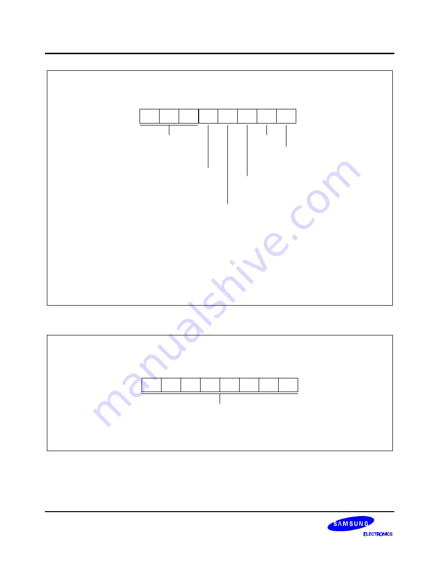
Oscillator Control Register (OSCCON)
F3H, Set 1, bank 0, R/W
.7
.6
.5
.4
.3
.2
.1
.0
MSB
LSB
Not used
System clock selection bit:
0 = Main oscillator select
1 = Subsystem oscillator select
Not used
Subsystem oscillator control bit:
0 = Subsystem oscillator RUN
1 = Subsystem oscillator STOP
Mainsystem oscillator control bit:
0 = Mainsystem oscillator RUN
1 = Mainsystem oscillator STOP
Subsystem oscillator driving
ability control bit:
0 = Strong driving ability
1 = Normal driving ability
NOTE:
In strong mode the warm-up time is less than 100 ms.
When the CPU is operated with fxt (sub-oscillation clock), it is possible to use the stop
instruction but in this case before using stop instruction, you must select fxx/128 for basic
timer counter clock input.
Then the oscillation stabilization time is 62.5 ((1/32768) x 128 x 16) ms + 100 ms
Here the warm-up time is from the time that the stop release signal activates to the time
that basic timer starts counting.
Figure 7-5. Oscillator Control Register (OSCCON)
STOP Control Register (STPCON)
F4H, Set 1,bank 0, R/W
.7
.6
.5
.4
.3
.2
.1
.0
MSB
LSB
STOP Control bits:
Other values = Disable STOP instruction
10100101 = Enable STOP instruction
Figure 7-6. STOP Control Register (STPCON)
Summary of Contents for C8245
Page 31: ...ADDRESS SPACES S3C8248 C8245 P8245 C8247 C8249 P8249 2 20 NOTES ...
Page 107: ...INTERRUPT STRUCTURE S3C8248 C8245 P8245 C8247 C8249 P8249 5 18 NOTES ...
Page 195: ...INSTRUCTION SET S3C8248 C8245 P8245 C8247 C8249 P8249 6 88 NOTES ...
Page 221: ...I O PORTS S3C8248 C8245 P8245 C8247 C8249 P8249 9 16 NOTES ...
Page 245: ...16 BIT TIMER 0 1 S3C8248 C8245 P8245 C8247 C8249 P8249 12 10 NOTES ...
Page 249: ...WATCH TIMER S3C8248 C8245 P8245 C8247 C8249 P8249 13 4 NOTES ...
Page 267: ...A D CONVERTER S3C8248 C8245 P8245 C8247 C8249 P8249 15 6 NOTES ...
Page 299: ...S3P8245 P8249 OTP S3C8248 C8245 P8245 C8247 C8249 P8249 21 8 NOTES ...
Page 307: ......
Page 309: ......
Page 311: ......
Page 313: ......