


Page 13 of 16 ft8_II_assy_smd_diode_072020.pdf
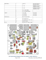
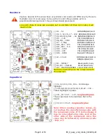
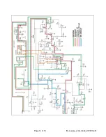
X-ray view of board. “floating” pads are connected to ground plane, not shown for clarity.
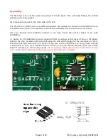
D=Drain G=Gate S=Source E=Emitter B= Base C=Collector I=Input G=Ground O=Output
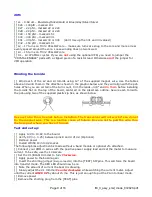
Pin
1
2
3
4
5
6
7
8
U1
1.42
1.42
0
7.15
7.15
8.3
7.5
8.35
U2 Rx 0
0
0
0
4.5
4.5
4.5
9
Rx
D / C
G / B
S / E
Tx
D / C
G / B S /E
Q1
0V
0V
0V
0V
9V
0V
Q2
0V
9V
0V
0V
0V
0V
Q4
9V
0V
0V
0V
9V
0V
Q6/7/8 9V
0V
0V
9V
~2.5V 0V
Q3
0V
0V
0V
0V
0.78V 0V
Q5
0V
9V
9V
8.8V
8.15V 9V