QRPGuys Digital DSB II Transceiver Kit Instructions Manual Download Page 11

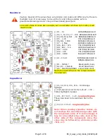
Page 11 of 16                                      ft8_II_assy_smd_diode_072020.pdf 

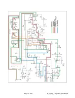
Theory of operation:


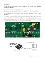
The Digital DSB transceiver is built around the ubiquitous SA602/612A mixer-oscillator chip. It 
provides both the receive and transmit functions.  
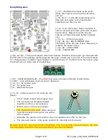
 

Receiver: 


The antenna is first routed through the transmitter's Low Pass Filter (LPF) and then into a BS170 
MOSFET,  which  is  the  receiver  input  T/R  switch.  The  received  signal  is  coupled  into  a  new  High 
Pass  Filter  (HPF)  circuit  comprised  of  C26  and  L1.  Stray  capacitance  (~88pF)  resonates  L1  to 
about the operating frequency.   
 
The received input signal is applied to the input of the SA602 mixer (U1) to produce the base line 
audio  output.  The  Local  Oscillator  is  either  the  crystal  on  the  band  module  using  the  internal 
oscillator of the SA602, or an optional Digital VFO.  
 
U2b,  one  half  of  a  LM358  op  amp,  provides  audio  gain  for  decent  sensitivity.  A  non-inverting 
configuration is used so that the input can be high impedance, allowing for reasonably small value 
input  coupling  caps.  The  gain  is  set  to  47.  The  amplifier  then  drives  an  audio  level  pot  so  the 
audio level can be adjusted to a level suitable for your PC sound card. Q1 provides muting of the 
audio output by shorting the input to the audio level pot to ground.  


Transmitter:


The SA602/612 requires very little input signal to saturate. Therefore a resistor divider is placed 
between the audio input from the sound card to the mixer input. This allows you to set the audio 
output from the sound card to a reasonable level and not overdrive the mixer.  
 
The other half of the LM358 (U2a) is used as a VOX circuit. The peak detector circuit of D3 and 
C12 isn't required for FT8 operation, but is included if one wishes to experiment with other modes 
where the audio input can drop to zero for short periods of time.  
 
The output of the Peak Detector activates the T/R switching. 


Q4 turns on, activating this sequence:   


Q2 is turned off, which disconnects the antenna from the mixer input.   


Q5 is turned on, which switches on the power to the transmit circuits.   


Q1 is turned on, muting the audio output.  


Q3 is turned on, shunting any transmit RF which might leak through Q1.  


Q6-Q7-Q8 amplifies the RF output from the mixer to a level sufficient to drive the PA. The PA is 
comprised of three BS170 MOSFETS in parallel. Bias is applied to the gates to place the amplifier 
into  linear  mode.  This  also  reduces  the  amount  of  drive  needed  since  the  input  signal  does  not 
have to first exceed the ~2.5V it takes to start to turn on the MOSFETS. The signal then goes to 
the Low Pass Filter (LPF) and finally the antenna.   
 
Power to the circuits is supplied by a 9V, 1A regulator. This ensures the power output remains in a 
safe operating area and if there is a problem, the internal over current protection will shut down 
the regulator.  Since the maximum operating voltage of the SA602/612 is 9V, a diode is placed in 
series  with  the  9V  supply  insure  the  voltage  to  the  chip  does  not  exceed  the  maximum 
recommended supply voltage. 


Summary of Contents for Digital DSB II Transceiver Kit

Page 1: ...ts List Location Quantity value Type C1 C2 C10 C13 C16 5 10 nF 103 X7R MMLC C3 C7 2 100 uF electrolytic 16V Long lead plus C4 C5 C6 C8 C9 C12 C14 C15 C18 C19 C20 C22 12 100 nF 104 X7R MMLC C11 C17 C21...

Page 2: ...MEG BRN BLK GRN GLD U1 1 SA602 or SA612A SO8 MIXER OSC U2 1 LM358 DIP8 DUAL OPAMP U3 1 LM7809 TO 220 9V 1A REG V1 V2 2 2K 6mm Trimmer resistor T1 T2 2 FT37 43 FERITE CORE BLACK DIP SOCKET 1 8 PIN DIP...

Page 3: ...2 uH RED RED GLD GLD or RED RED GLD SIL 4 T37 2 RED CORES 2 T37 6 YELLOW CORES crystals 1 7 074 MHz HC 49 US 1 10 136 MHz HC 49 US 1 14 074 MHz HC 49 US Miscellaneous 3 Band module boards 12 1 26 magn...

Page 4: ...ite smd soldering method or we have found the process below to be quite satisfactory Solder U1 the SA602 612 smd component first by wiping a thin layer of flux on the board position the chip carefully...

Page 5: ...1 R20 5 6 GRN BLU GLD GLD R13 470K YEL VOL YEL GLD R14 47K YEL VOL ORG GLD R15 680K BLU GRY YEL GLD L4 10 uH BRN BLK BLK GLD or BRN BLK BLK SIL D1 1N5817 Black plastic body D2 D3 1N4148 Small Glass bo...

Page 6: ...t of the board Make U shaped pieces of resistor lead clippings to hold the body of the BS170 s to the board using the small holes on either side of the package D4 CLEAR LENS RED LED the short lead goe...

Page 7: ...three band modules and detailed the values for 20 30 40m Additional bare band module pcb s are available for operation on other bands At the end of this document we have modeled additional band compo...

Page 8: ...L2 20 turns on T37 2 RED core make sure turns are snug to the core and more or less evenly spaced around the core Loose winding does not work well L3 18 turns on T37 2 RED core X1 7 074 MHz crystal I...

Page 9: ...top of the board centered on the silkscreen outline Secure each toroid to the pcb using two of the supplied plastic zip ties as shown below Be sure to tin the wire ends before installing The transceiv...

Page 10: ...card output level until the board switches into Transmit RED LED goes on you can continue to increase the output level a little bit to ensure reliable triggering of the VOX circuit If you have a watt...

Page 11: ...card to the mixer input This allows you to set the audio output from the sound card to a reasonable level and not overdrive the mixer The other half of the LM358 U2a is used as a VOX circuit The peak...

Page 12: ...nd your meter Only be concerned if the voltages are significantly different than those shown Almost all of the construction issues with the DSB transceiver have been traced to the faulty installation...

Page 13: ...Drain G Gate S Source E Emitter B Base C Collector I Input G Ground O Output Pin 1 2 3 4 5 6 7 8 U1 1 42 1 42 0 7 15 7 15 8 3 7 5 8 35 U2 Rx 0 0 0 0 4 5 4 5 4 5 9 Rx D C G B S E Tx D C G B S E Q1 0V...

Page 14: ...Page 14 of 16 ft8_II_assy_smd_diode_072020 pdf...

Page 15: ...Page 15 of 16 ft8_II_assy_smd_diode_072020 pdf...

Page 16: ...___________________ _________________________________________________ _________________________________________________ _________________________________________________ ______________________________...

Reviews: