background image


UC10.241, UC10.242


UC-Series 

24V,


15A,


CAPACITOR-BASED


DC-UPS 


I

NDEX


 Page 

Page

1.


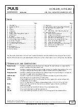
Intended Use .......................................................3


2.


Installation Notes ................................................3


3.


Input ....................................................................4


4.


Output .................................................................5


5.


Charging ..............................................................7


6.


Buffer Time..........................................................8


7.


Ready and Buffering Relay Contact ...................9


8.


Inhibit Input.........................................................9


9.


PC-Mode ............................................................10


10.


Efficiency and Power Losses..............................11


11.


Lifetime Expectancy and MTBF.........................12


12.


Functional Diagram...........................................13


13.


Terminals and Wiring........................................14


14.


Front Side and User Elements...........................15


15.


EMC....................................................................16


16.


Environment ......................................................17


17.


Protection Features ...........................................18


18.


Safety Features ..................................................18


19.


Approvals .......................................................... 19


20.


RoHS, REACH and Other Fulfilled Standards .. 19


21.


Physical Dimensions and Weight ..................... 20


22.


Accessories ........................................................ 21


22.1.


ZM2.WALL – Wall-Mounting Bracket ......21


23.


Application Notes............................................. 22


23.1.


External Input Protection.........................22


23.2.


Output Circuit Breakers............................22


23.3.


Parallel Use to Increase Output Current..22


23.4.


Parallel Use for Redundancy ....................23


23.5.


Parallel Use for Longer Buffer Times.......23


23.6.


Series Use for 48V Applications ...............24


23.7.


Using the Inhibit-Input.............................24


23.8.


External Controlled Delayed Shut-down.25


23.9.


What do KJ and KWS mean? ...................26


23.10.


Troubleshooting .......................................27


The information presented in this document is believed to be accurate and reliable and may change without notice. 

No part of this document may be reproduced or utilized in any form without permission in writing from the publisher. 


T

ERMINOLOGY AND 

A

BREVIATIONS


Normal mode


Describes a condition where the capacitor is charged, the input voltage is in range and the 
output is loaded within the allowed limits. 

Buffer mode


Describes a condition where the input voltage is below the transfer threshold level, the unit is 
running on capacitor (buffering) and the output is loaded within the allowed limits. 

Charging mode 

Describes a condition where the capacitor is being charged, the input voltage is in range and 
the output is loaded within the allowed limits. 

Inhibit mode 

Describes a condition where buffering is disabled on purpose (e.g. for service actions) 

T.b.d.


To be defined, value or description will follow later. 

AC 24V 

A figure displayed with the AC or DC before the value represents a nominal voltage with 
standard tolerances included.  
E.g.: DC 12V describes a 12V battery disregarding whether it is full (13.7V) or flat (10V) 

24Vac 

A figure with the unit (Vac) at the end is a momentary figure without any additional 
tolerances included.  

may


A key word indicating flexibility of choice with no implied preference. 

shall


A key word indicating a mandatory requirement. 

should


A key word indicating flexibility of choice with a strongly preferred implementation. 

May 2016 / Rev. 2.2 DS-UC10.241-EN 
All parameters are specified at 24V, 10A output current, 25°C ambient and after a 5 minutes run-in time unless otherwise noted. 

www.pulspower.com   Phone +49 89 9278 0    Germany 

2/27

Summary of Contents for DIMENSION UC Series

Page 1: ...t this energy is released to the DC bus in a regulated process The DC UPSs are maintenance free and have a similar lifetime expectancy as power supplies No regular replacement of the capacitors is nec...

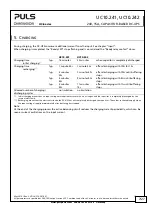
Page 2: ...he publisher TERMINOLOGY AND ABREVIATIONS Normal mode Describes a condition where the capacitor is charged the input voltage is in range and the output is loaded within the allowed limits Buffer mode...

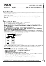
Page 3: ...permanently with more than 50 of the rated power Increase this clearance to 15mm in case the adjacent device is a heat source e g a power supply Fig 2 1 Typical wiring diagram buffered branches non b...

Page 4: ...A buffer current The transfer threshold voltage describes the input voltage where the unit switches into buffer mode and delivers output voltage from the capacitors if the input was above the turn on...

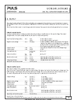
Page 5: ...15A see Fig 4 2 Short circuit current min 17 9A load impedance 100mOhm see Fig 4 2 max 21 0A load impedance 100mOhm see Fig 4 2 Output capacitance typ 1 500 F included inside the DC UPS Capacitive an...

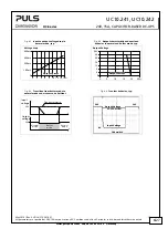
Page 6: ...8 12 14 200mv 300mv Voltage drop Fig 4 3 Transition from buffer mode to normal mode and vice versa definitions Fig 4 4 Transfer behavior typ 500ms DIV 0V Output Voltage Input Voltage 24V 22 25V at 10...

Page 7: ...after discharging with 1A until buffering stops Allowed number of charging discharging cycles no limitation no limitation Initial charging means that no input voltage was applied for several hours or...

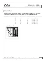
Page 8: ...680s at 0 5A buffer current typ 200s 400s at 1A buffer current typ 68s 136s at 3A buffer current typ 39s 78s at 5A buffer current typ 26s 53s at 7A buffer current typ 16 5s 33s at 10A buffer current...

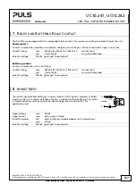
Page 9: ...ad min 1mA at 5Vdc min permissible load Isolation voltage 500Vac signal port to power port 8 INHIBIT INPUT The inhibit input disables buffering In normal mode a static signal is required In buffer mod...

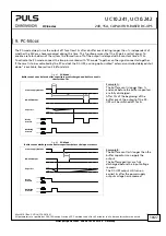
Page 10: ...Power Supply Output DC UPS Output full empty Capacitor Ready Contact closed open Buffering Contact closed open 5s 70s Example A The buffer event is longer than 1s and ends before the buffer capacitors...

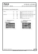
Page 11: ...pacitor fully charged typ 5 0W During charging 0A output current Fig 10 1 Efficiency vs output current in normal mode typ Fig 10 2 Power losses vs output current in normal mode typ Power losses versus...

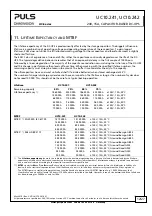
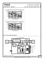
Page 12: ...10A 55 C 19 000h 34 000h 19 000h 34 000h at 24V 15A 55 C MTBF UC10 241 UC10 242 MTBF SN 29500 IEC 61709 1 519 000h 1 515 000h at 24V 10A 25 C 1 443 000h 1 439 000h at 24V 15A 25 C 899 000h 895 000h a...

Page 13: ...9 50 A Remaining capacity A 85 B 75 B 15A Output Current 12 FUNCTIONAL DIAGRAM Fig 12 1 Functional diagram 24V Power Supply Boost Converter Step up Converter Charger Balancing Safety Circuits Input E...

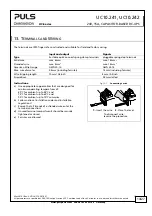
Page 14: ...onnecting a wire Instructions a Use appropriate copper cables that are designed for minimum operating temperatures of 60 C for ambient up to 45 C and 75 C for ambient up to 60 C and 90 C for ambient u...

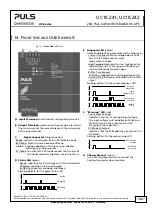
Page 15: ...Flashing pattern for the red warning LED Check input voltage 1 0 1 0 PC Mode activated AUU Input Terminals quick connect spring clamp terminal UUBUU Output Terminals quick connect spring clamp termina...

Page 16: ...coupling clamp Criterions A DC UPS shows normal operation behavior within the defined limits EMC Emission According generic standards EN 61000 6 3 and EN 61000 6 4 Conducted emission IEC CISPR 16 1 2...

Page 17: ...2103 EN 50178 not conductive LABS compatibility The unit does not release any silicone or other LABS critical substances and is suitable for use in paint shops Operational temperature is the same as t...

Page 18: ...ve balancing circuit ensures uniform capacitor voltages If necessary the charging current will be reduced to a safe value Failing of one or more capacitor in the capacitor string included Ready contac...

Page 19: ...TEX certificate EPS 15 ATEX 1 025 X The power supply must be built in in an IP54 enclosure EN 60079 0 EN 60079 15 ATEX II 3G Ex nA nC II T4 Gc Suitable for use in Class 1 Zone 2 Groups IIa IIb and IIc...

Page 20: ...The DIN rail height must be added to the unit depth 127mm to calculate the total required installation depth Installation Clearances See chapter XX2XX Fig 21 1 Front view UC10 241 Fig 21 2 Front view...

Page 21: ...s bracket is used to mount the DC UPS onto a flat surface without utilizing a DIN Rail UC10 241 UC10 242 May 2016 Rev 2 2 DS UC10 241 EN All parameters are specified at 24V 10A output current 25 C amb...

Page 22: ...the wire size that is used the wiring is considered as thermally safe regardless of whether the MCB opens or not To avoid voltage dips and under voltage situations in adjacent 24V branches which are s...

Page 23: ...2 Wiring example for a fully redundant system redundant power supplies and redundant DC UPSs Power Supply 24V Output Power Supply 24V Output Load Failure Monitor YRM2 DIODE OUT IN 1 IN 2 IN 1 IN 2 23...

Page 24: ...tic signal is required In buffer mode a pulse with a minimum length of 250ms is required to stop buffering The inhibit signal is stored and can be reset by cycling the input voltage For service purpos...

Page 25: ...ontact closed External signal to start the delayed shut down Load open closed Buffering Contact open 1s full empty Capacitor Pin 7 8 open Ready Threshold 250ms Activation of the external control mode...

Page 26: ...depends on the load current the lower the load current the lower the cut off voltage Considering this voltage range the energy can be calculated with the following formula full charge voltage U1 2 5V...

Page 27: ...ee notes in section 2 first Symptom Action Check input voltage LED is on Check input voltage must be between 22 8V and 30V DC UPS did not buffer Inhibit input was set Capacitor did not have enough tim...

Reviews: