


Rev. A 10/18
24
Application Note
AN-72
www.power.com
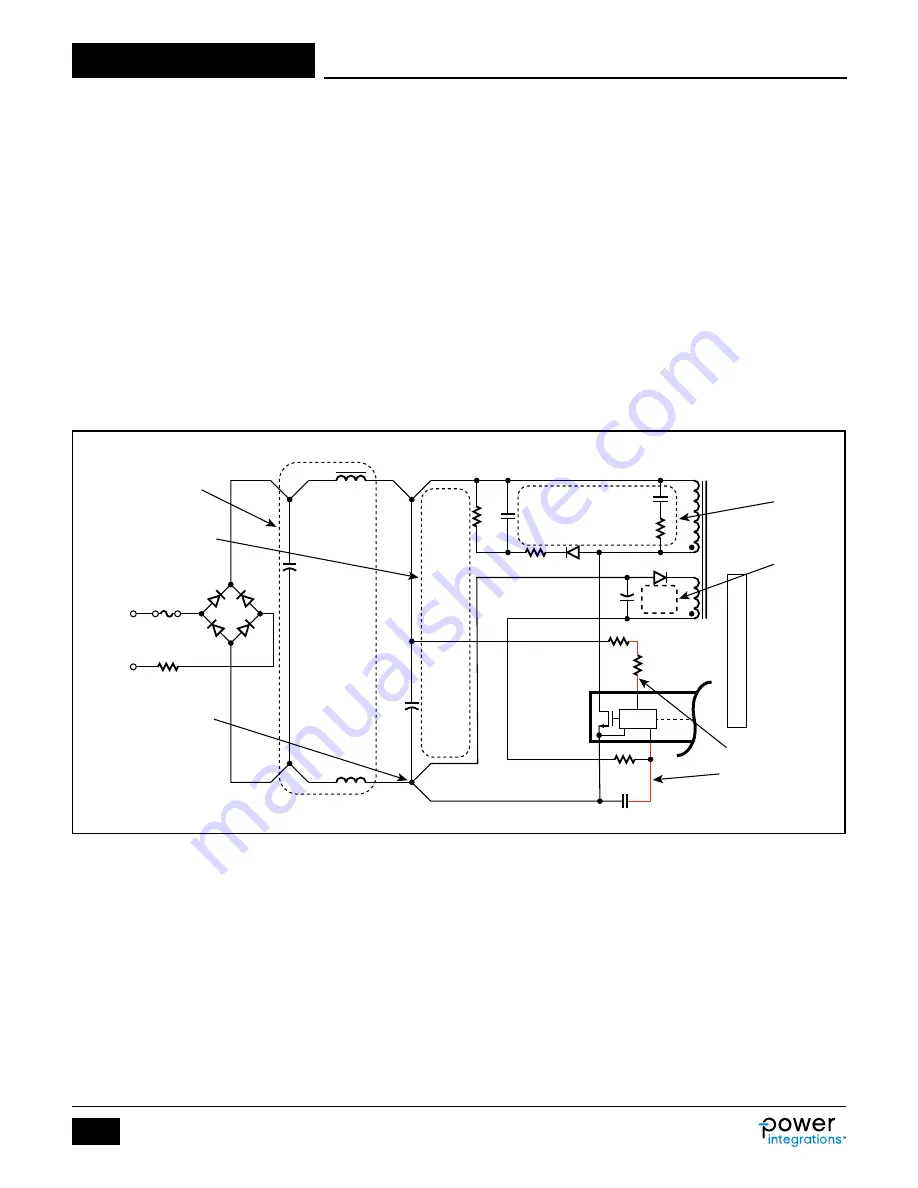
Figure 20. Typical Schematic of InnoSwitch3 Secondary-Side Showing Critical Loops Areas, Critical Component Traces and Single-Point or Star Grounding.
Optional Post Filter LC included.
PI-8467a-103017
L
R
T
F
R
C1
C2
R
SN
C
SN
C
P
R
P
N
P
N
B
T
R
S
D
SN
D
BIAS
R
BP
R
LS
R
LS1
C
BPP
C
BIAS
N
Primary FET
and Controller
PRIMARY
D
V
S
BPP
InnoSwitch3
t
O
L
F
F
B
BRD
S
E
C
O
N
D
A
R
Y
2
1
L
F
, C1 and F
B
should be
positioned away from any
switching nodes with high
di/dt or dv/dt
Primary clamp loop
area (2) must be tight
and small as possible
Red lines denote as short
as possible and as close
as possible to IC pins
Bias supply loop
area (3) must be tight
and small as possible
Primary loop area (1) formed
by C2, N
P
and D-S pins must
be tight and small as possible
Single-point or star-ground
connection; ground traces
for bias supply and SOURCE
pin are separated and
connected to a single-point
at C2 node
3
Y Capacitor
The placement of the Y capacitor should be directly from the primary
input filter capacitor positive terminal to the output positive or return
terminal of the transformer secondary. Such a placement will route
high magnitude common mode surge currents away from the IC.
Note that if an input pi EMI filter C1, L
F
, C2 is used, then the inductor
in the filter should be placed between the negative terminals of the
input filter capacitors.
Output SR MOSFET
For best performance, the area of the loop connecting the secondary
winding, the output SR MOSFET, and the output filter capacitor
should be minimized. In addition, sufficient copper area should be
provided at the terminals of the SR MOSFET for heat sinking. The
distance between SR FET source and InnoSwitch3 GROUND pin
needs to be short. To prevent negative current flowing through the
primary MOSFET.
ESD Immunity
Sufficient clearance should be maintained (>8 mm) between the
primary-side and secondary-side circuits to enable easy compliance
with any ESD or hi-pot isolation requirements. The spark gap is best
placed between output return and/or positive terminals and one of
the AC inputs (after the fuse). In this configuration a 6.4 mm (5.5
mm is acceptable – dependent on customer requirement) spark gap
is more than sufficient to meet the creepage and clearance
requirements of most applicable safety standards. This is less than
the primary to secondary spacing because the voltage across spark
gap does not exceed the peak of the AC input. See layout example
Figure 21.
A spark gap across the common-mode-choke or inductor helps
provide low impedance path for a high energy discharge due to ESD
or a common-mode surge.
Drain Node
The drain switching node is the dominant noise generator. As such
the components connected the drain node should be placed close to
the IC and away from sensitive feedback circuits. The clamp circuit
components should be located physically away from the PRIMARY
BYPASS pin, and the trace width and length in this circuit should be
minimized.