


Rev. A 10/18
23
Application Note
AN-72
www.power.com
close as possible to the SOURCE and PRIMARY BYPASS pins of the
device.
Primary sensed OVP can be realized by connecting a
series
combination of a Zener diode, a resistor and a blocking diode from
the rectified and filtered bias winding voltage supply to the PRIMARY
BYPASS pin (see Figure 18-a). The rectified and filtered bias winding
output voltage may be higher than expected (up to 1.5X or 2X the
desired value) dependent on the coupling of the bias winding with the
output winding and the resulting ringing on the bias winding voltage
waveform. It is therefore recommended that the rectified bias
winding voltage be measured. Ideally this measurement should be
made at the lowest input voltage and with full output load. This
measured voltage should be used to select the components required
to provided primary sensed OVP. It is recommended that a Zener
diode with a clamping voltage approximately 6 V lower than the bias
winding rectified voltage at which OVP is expected to be triggered be
used. A forward voltage drop of 1 V can be assumed for the blocking
diode. A small signal standard recovery diode should be used. The
blocking diode prevents any reverse current charging the bias
capacitor during start-up. Finally, the value of the series resistor set
such that a current higher than I
SD
will flow into the PRIMARY BYPASS
pin during an output overvoltage event.
Secondary-Side Overvoltage Protection
Secondary-side output overvoltage protection is provided by the
InnoSwitch3 IC. It is activated when an internal auto-restart is
triggered when a current exceeding the I
BPS(SD)
threshold is fed into
the SECONDARY BYPASS pin. The direct output sensed OVP function
can be realized by connecting a Zener diode from the output to the
SECONDARY BYPASS pin. The Zener diode voltage rating shall be the
difference between 1.25 V
OUT
and 4.4 V SECONDARY BYPASS pin
voltage. It is necessary to add a low value resistor, in series with the
OVP Zener diode to limit the maximum current into the SECONDARY
BYPASS pin (see Figure 18-b).
An OVP for a 5 V output can be implemented by two-diodes in series
(shown in Figure 18-c). The filter capacitor should be rated for 6.3 V.
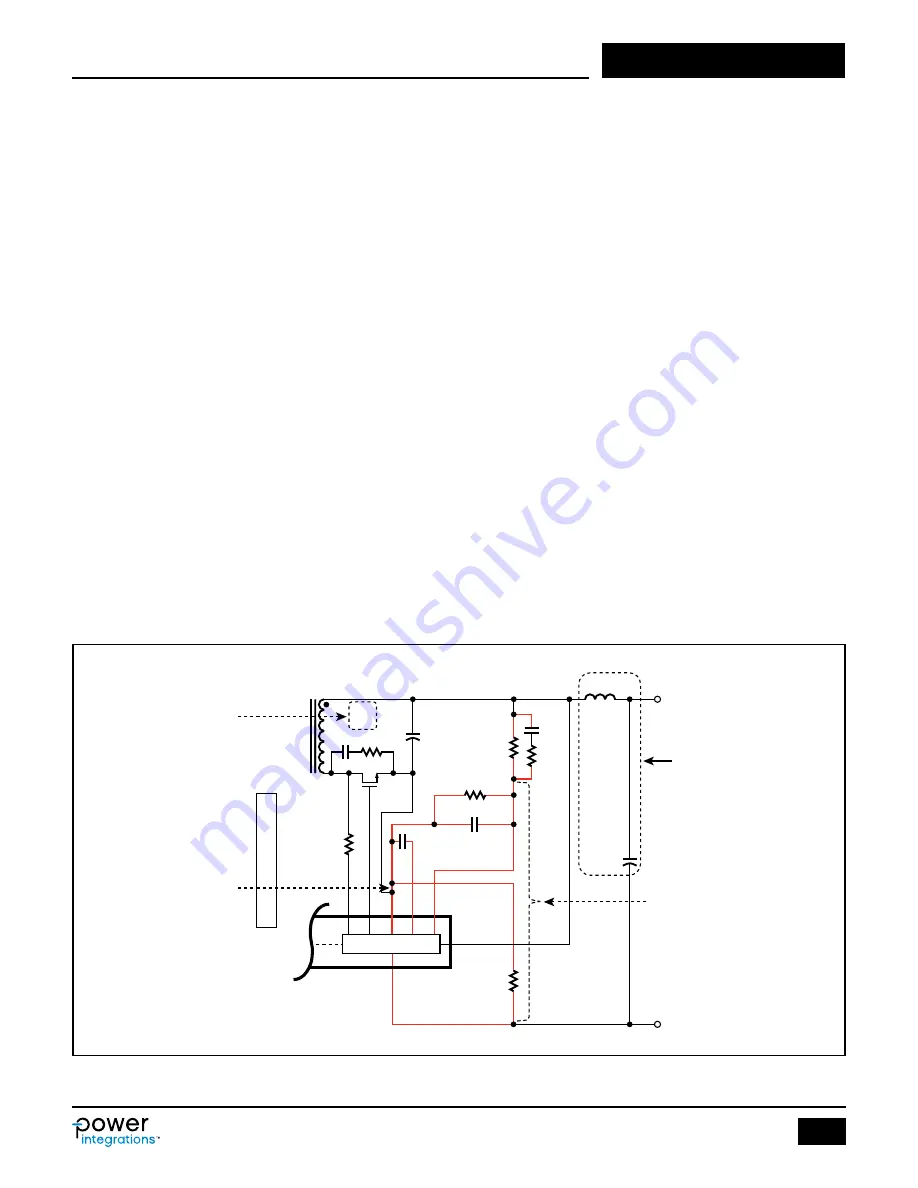
Recommendations for Circuit Board Layout
Single-Point Grounding
Use a single-point ground connection from the input filter capacitor to
the area of copper connected to the SOURCE pin. See Figures 19 and
20.
Bypass Capacitors
The PRIMARY BYPASS (C
BPP
), SECONDARY BYPASS (C
BPS
) decoupling
capacitors must be located directly adjacent to the PRIMARY
BYPASS-SOURCE, SECONDARY BYPASS-GROUND and FEEDBACK-
GROUND (C
FB
) pins respectively and connections should be routed via
short traces.
Signal Components
External components R
LS
, R
BP
, R
FB(UPPER)
, R
FB(LOWER)
and R
IS
which are
used for monitoring feedback information must be placed as close as
possible to the IC pin with short traces.
Critical Loop Area
Circuits where high dv/dt or di/dt occurs should be kept as small as
possible. The area of the primary loop that connects the input filter
capacitor, transformer primary and IC should be kept as small as
possible.
No loop area should be placed inside another loop (see Figure 21).
This will minimize cross-talk between circuits.
Primary Clamp Circuit
A clamp is used to limit peak voltage on the DRAIN pin at turn-off.
This can be achieved by using an RCD clamp or a Zener diode (~200 V)
and diode clamp across the primary winding. To reduce EMI, minimize
the loop between the clamp components, the transformer and the IC.
PI-8466a-111017
Secondary
Control IC
V
OUT
RTN
R
FB(UPPER)
R
FB(LOWER)
R
PH
R
IS
C
PH
C
PF
C
FB
C
BPS
C
SR
4
R
SR
C
OUT
R
FWD
SR FET
IS
VOUT
BPS
FB
GND
SR
FWD
L
PF
P
R
I
M
A
R
Y
N
S
T
Secondary loop area (4)
formed by NS, C
OUT
and
SR-FET must be tight
and small as possible
If used, post filter L
PF
and
C
PF
must be as close as
possible to output terminals
Note that Feedback network
(i.e. R
FB(UPPER)
) and V
OUT
pin
must be connected before the
post filter inductor L
PF
Red lines denote the trace
must be as shorts as possible
and as close as possible to
IC pins
Single-point or Star-Ground
connection; Ground traces
for GND pin, C
OUT
, and
Feedback components are
separated and star-connected
to a single point at R
IS
node
Figure 19. Typical Schematic of InnoSwitch3 Primary-Side Showing Critical Loops Areas, Critical Component Traces and Single-Point or Star Grounding.