


Rev. A 10/18
18
Application Note
AN-72
www.power.com
External Bias Supply Components (D
BIAS
, C
BIAS
, R
BP
)
The PRIMARY BYPASS pin has an internal regulator that charges the
PRIMARY BYPASS pin capacitor to V
BPP
by drawing current from the
DRAIN pin whenever the power MOSFET is off. The PRIMARY
BYPASS pin is the internal supply voltage interface node. When the
power MOSFET is on, the device operates from the energy stored in
the PRIMARY BYPASS pin capacitor. In addition, a shunt regulator
clamps the PRIMARY BYPASS pin voltage to V
SHUNT
when current is
provided to the PRIMARY BYPASS pin through an external resistor.
This allows the InnoSwitch3 to be powered externally through a bias
winding, decreasing the no-load consumption to less than 15 mW in a
5 V output design.
12 V is the recommended bias voltage. Higher voltage will increase
no-load input power. Ultrafast diodes are recommended for the bias
winding rectifier to reduce no-load power consumption.
A 22
µ
F, 50 V low ESR electrolytic aluminum capacitor is recommended
for the bias supply filter, C
BIAS
. A Low ESR electrolytic capacitor will
reduce no-load input power. Use of ceramic surface mount capacitor
is not recommended as they cause audible noise due to piezoelectric
effect in its mechanical structure.
To have the minimum no-load input power and high full load power
efficiency, Resistor R
BP
should be selected such that the current
through this resistor is higher than the PRIMARY BYPASS pin current.
The
PRIMARY BYPASS
pin supply current at normal operating
frequency can be calculated as shown in the following equation;
I
kHz
F
I
I
I
132
SSW
SW
S
S
S
2
1
1
#
=
-
+
^
h
Where;
I
SSW
: PRIMARY BYPASS pin supply current at operating switching
frequency
F
SW
: Operating switching frequency (kHz)
I
S1
: PRIMARY BYPASS pin supply current at no switching
(refer to data sheet)
I
S2
: PRIMARY BYPASS pin supply current at 132 kHz
(refer to data sheet)
The BPP voltage is internally clamped to 5.3 V when bias current is
higher than PRIMARY BYPASS pin supply current. If BPP voltage is
~5.0 V, then this indicates that the current through R
BP
is less than
the PRIMARY BYPASS pin supply current and charge current is being
drawn from the DRAIN pin to keep the PRIMARY BYPASS pin above
5.0 V except during start-up.
To determine maximum value of R
BP
;
/
.
R
V
V
I
V
V
5 3
;
BP
BIAS NO LOAD
BPP
SSW
BPP
-
=
-
^
h
6
@
=
Output Synchronous Rectifier MOSFET (SR FET)
InnoSwitch3 features a built-in synchronous rectifier (SR) driver that
enables the use of low-cost low voltage MOSFETs for synchronous
rectification and increases system efficiency. Since the SR driver is
referenced to the output GND, the SR FET is placed in the return line.
GND is the typical threshold that ensures the SR FET will turn off
(V
SR(TH)
) at the end of the flyback conduction time. There is a slight
delay between the commencement of the flyback cycle and the
turn-on of the SR FET in order to avoid current shoot through.
During SR FET conduction the energy stored in the inductor is
transferred to the load, the current will continue to drop until the
voltage drops across the R
DS(ON)
of the SR FET drops to 0 V, at this point
the SYNCHRONOUS RECTIFIER pin will pull the gate low to
instantaneously turn off the SR FET. Minimal current will flow
through the SR FET body diode during the remainder of the flyback
time (see Figure 15). Putting a schottky diode across the SR FET may
further increase efficiency by 0.1% − 0.2% depending on the design
and SR FET used. In continuous conduction mode (CCM), the SR FET
is turned off when a feedback pulse is sent to the primary to demand
a switching cycle, providing excellent synchronous operation, free of
any cross conduction between the SR FET and primary MOSFET.
The SR FET driver uses the SECONDARY BYPASS pin for its supply
rail, and this voltage is typically 4.4 V. A SR FET with a high threshold
voltage is therefore not suitable. SR FETs with a gate voltage
threshold voltage range (V
G(TH)
) of 1.5 V to 2.5 V are recommended.
Since the termination of the ON-time of the SR FET is based on when
the Drain-Source voltage of the MOSFET reaches to 0 V during the
conduction cycle using an SR MOSFET with ultra-low R
DS(ON)
(< 5 m
Ω
)
may result to early termination of the SR FET drive signal. This will
cause secondary current to conduct instead through its body diode,
which has a higher voltage drop compared to the SR FET’s R
DS(ON)
which will slightly reduce system efficiency (see Figure 16).
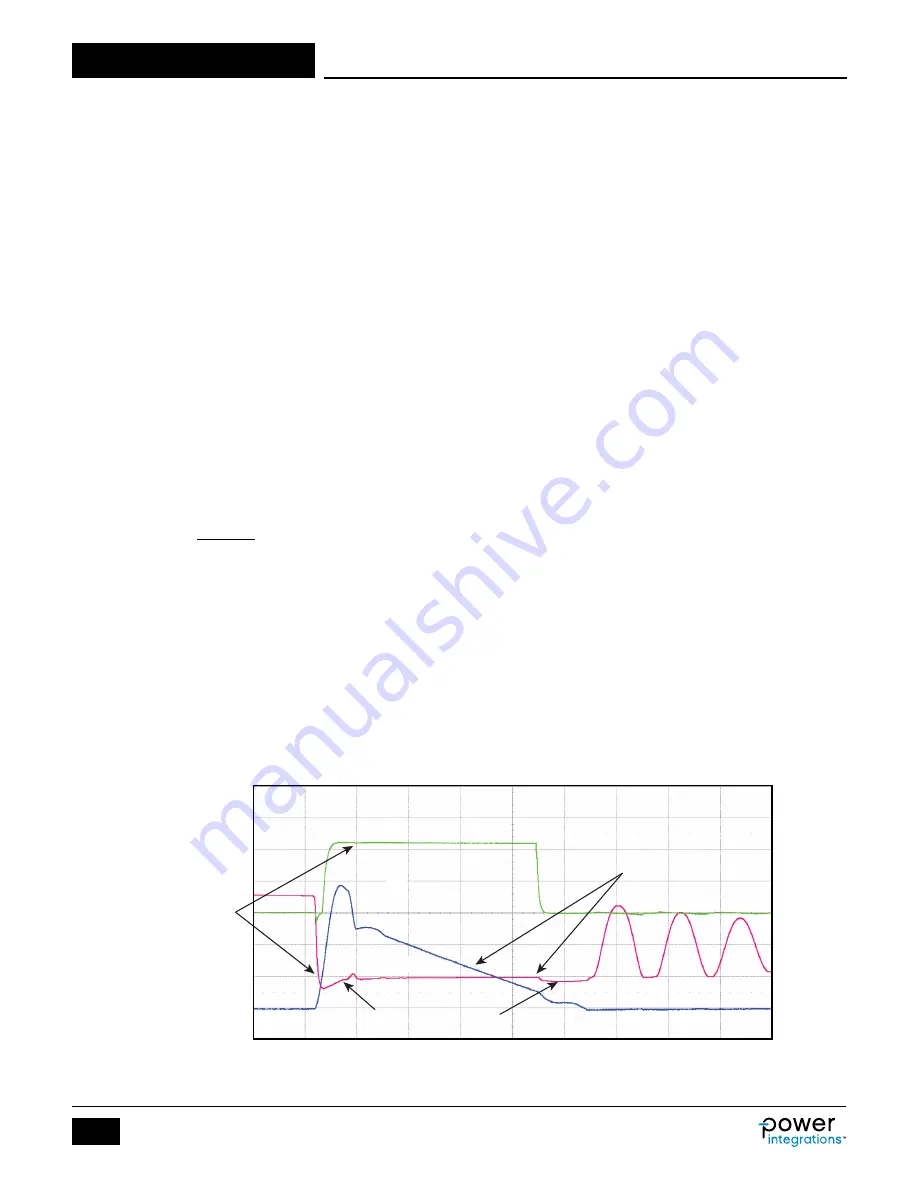
Figure 15. SR FET Turn-ON and Turn-OFF Events During DCM Operation.
Forward voltage
falls below 0 V,
the SR FET turned on
after ~500 ns delay
SR FET is off, current flows
through the body diode,
voltage drop increases
As diode current falls,
voltage drop across R
DS(ON)
approaches zero
SR Gate
Drive
Diode
Current
Forwad
Voltage
PI-8514-091318
V
GS
I
DS
V
DS