


Rev. A 10/18
21
Application Note
AN-72
www.power.com
output power. The actual rating of the capacitor will therefore
depend on the peak-to-average power ratio of the design. In most
cases, this assumption will be valid as capacitor ripple rating is a
thermal limitation and most peak load durations are shorter than the
thermal time constant of the capacitor (typically < 1 s).
In either case, if a suitable capacitor cannot be found then
two or
more capacitors may be used in parallel to achieve a combined ripple
current rating equal to the sum of the individual capacitor ripple
ratings. Many capacitor manufacturers provide factors that increase
the ripple current rating as the capacitor operating temperature is
reduced from its data sheet maximum. This is to ensure that the
capacitor is not oversized.
The use of aluminum-polymer solid capacitors has gained
considerable
popularity due to their compact size, stable temperature characteristics,
extremely low ESR and high RMS ripple current rating. These
capacitors enable the design of ultra-compact chargers and adapters.
Typically, 200
µ
F to 300
µ
F of aluminum-polymer capacitance per
ampere of output current is adequate. The other factor that
influences choice of the capacitance is allowable output ripple.
Ensure that only capacitors with a voltage rating higher than the
highest output voltage plus suitable margin are used.
The switching ripple voltage is equal to the peak secondary current
multiplied by the ESR of the output capacitor. It is therefore
important to select low ESR capacitor types to reduce the ripple
voltage. In general, selecting a high ripple current rated capacitor
results in an acceptable value of ESR.
The voltage rating of the capacitor should be at least 1.2 times the
output voltage (VOUT).
Output Current Sense Resistor (R
IS
)
For constant current (CC) output operation, the external current
sense resistor R
IS
should be connected between the IS pin and
secondary GROUND pin of the IC. If constant current (CC) regulation
is not required, the IS pin should be connected directly to the
GROUND pin of the IC.
The voltage generated across the resistor is compared to an internal
current limit voltage threshold (I
SV(TH)
) of approximately 35 mV.
The external current sense resistor R
IS
can be estimated by using;
/
R
I
I
IS
SV TH
OUT CC
=
^
^
h
h
The voltage developed across the resistor is connected to an internal
reference V
SV(TH)
(35 mV), the R
IS
resistor must be placed close to IS
and GROUND pins with short traces in order to prevent ground
impedance noise instability in constant current operation.
Output Post Filter Components (L
PF
, C
PF
)
If necessary a post filter (L
PF
and C
PF
) can be added to reduce high
frequency switching noise and ripple. Inductor L
PF
should be in the
range of 1
µ
H – 3.3
µ
H with a current rating above the peak output
current. Capacitor C
PF
should be in the range of 100
µ
F to 330
µ
F
with a voltage rating ≥ 1.25
×
V
OUT
. If a post filter is used then the
output voltage sense resistor should be connected before the post
filter inductor.
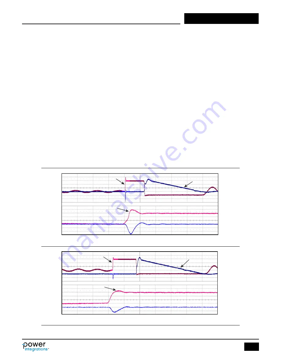
Figure 17. Effect of Body Diode Reverse Recovery Time on V
DS
.
SR FET with slow body diode, showing high-voltage spike, 17 V.
SR FET with fast body diode, significantly low voltage spike, 8 V.
PI-8517-100118
17 V Spike
SR FET Voltage Waveform, 20 V / div
SR FET Current Waveform, 2 A / div
PI-8518-100118
8 V Spike
SR FET Voltage Waveform, 20 V / div
SR FET Current Waveform, 2 A / div