background image

PDP-501MX, PDP-V501X

80

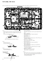
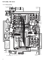
Note: Form the cables from the address module without touching the long leads of the pump up assembly as much as possible.

PA1

PA2

T1

T2

T3

D10

D11

D12

T7

T10

O3

O8

CG3

CG5

CG2

CG1

O2

O1

T15

T8

T11

T9

T12

L3

L6

L4

L7

L5

L8

H2

H9

H6

H1

D9

E8

H3

O4

O9

CG4

CG6

T13

T14

O5 O6 O7

T4 T5 T6

L2

L1

H7

H11

R3349

J101

J111

J109

J112

H10

H8

H12

Q2

CH2

Q1

CH1

K15

M5

M8

M4

M7

M3

M6

K9

K12

K8

K11

K7

K10

Q4

Q9

CH4

CH6

Q3

Q8

CH3

CH5

3

9

6

1

2

4

H4

5

H5

Q5 Q6 Q7

K4 K5 K6

M2

K13

M1

K14

7

10

8

K1

K2

K3

E11

E10

E9

Y DRIVE B

Y DRIVE A

X DRIVE A

X DRIVE B

CABLE H

CABLE F

F12

G9

F8

G7

F7

G6

F6

G5

F10

J110

F1

D8

G8

G9

F20

F18

F19

F17

G18

G16

G17

G15

CABLE D

U-CON

CABLE C

CABLE G

CABLE E

CABLE B

DIGITAL VIDEO

CABLE A

PB1

PB2

PD2

PF2

PD1

PF1

E3

E1

D2

D3

E4

D4

E5

D5

E6

D6

E7

D7

E2

E18

E17

E12

E13

D1

D15

D14

D13

E19

E14

E16

HEAT SINK

J108

J103

J113

J310

PF1

PF2

PD1

PD2

PB1

PB2

PB1

PB2

PB1

PB2

PA1

PA2

PA1

PA2

PC1

PC2

PA1

PA2

PE1

PE2

PE1

PE2

PC1

PC2

PA1

PA2

PA1

PB1

PA2

PB2

PB1

PB2

BIND

Q

BIND

U

BIND

X

BIND

V

BIND

W

BIND

L

BIND

Y

BIND

G

BIND

P

BIND

H

BIND 

I

BIND

E

BIND

R

BIND

F

BIND

T

Blue

Red

To fan

From
SIDE SWITCH

To fan

Black tape

Red

Red

Red

Red

Note2

Note2

Note2

Note4

Note2

Note3

Note

Do not touch 
the heat sink.

Hold the binders so that 
they become parallel.

Pull bind 

E

 so that it does not get 

caught by the fan motor.

Move the wires to the assembly side using binds 

G

 and 

Q

.

Pull with bind 

R

 so that 

it does not touch R3349.

Pass through the hole on 
the side of the sub-frame.

Pass through the hole on 
the side of the sub-frame.

Pass through the hole on 
the side of the sub-frame.

B3

B2

B4

Wire outside E2

Wire inside E17 and E18

Pull the shield wire from RGB  A6 .

To C1

Wire outside 

I

 8

Note2

Make sure (J109, J110) do not get caught 
when attaching the canter frame (2F) 
(when tightening the screws).
Branch the wires to 2F to the left and right 
from the center frame.
(Right : Red wire, Left : Blue wire)

3D Y/C

Note 1

Bend the flexible cables between the pump up assembly and the
cable assembly side at the cable assembly side, and close the
cover.
(To prevent the damage of the cover.)

Note 2

Bend the flexible cable.
(To prevent touching the frame.)

Bend to make parallel to the connector, and close.

Note 3

Bend the flexible cable.
(To prevent touching the fan.)

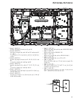
Bind 

R

 (AEP-215)

Pull in the 

]

 direction so that J111 does not touch R3349, and

bind.

Bind 

I

 (AEP-215)

Pull J109 and J112 in the 

]

 direction, and bind.

Bind 

W

 (AEP-215)

Bind the J310.

Bind 

E

 (AEP-215)

Pull in the 

]

 direction so that the wire of J109 to T15 does not

touch the fan, and bind.

Bind 

G

Q

L

 (AEP-215)

Pull J110 in the 

]

 direction, and bind.

Bind 

H

 (AEP-215)

Pull J110 and J103 in the 

]

 direction, and bind.

Bind 

F

 (AEP-215)

Bind 

T

 (AEC-826)

Secure the flexible cable so that it does not touch the fan.

Bind 

P

 (AEC-826)

Secure the flexible cable to distance from the 2F assembly.
(To prevent sub field noise.)

Bind 

U

V

 (AEP-215)

Pull J110 in the 

]

 direction and bind.

Bind 

U

 and 

V

 is temporary secure.

Note 4:

Pull the shield wires to D1 in the arrow direction (

|

) so that

they are away from the panel shield and bind with binds 

G

 and

Q

 along the board as much as possible.

(To prevent sub field noise)

Connector

Pump up assembly

Cable assembly

Connector

Flexible cable

Connector

Flexible cable

Connector

Bend at the blue line

of the flexible cable.

Digital video assembly

Bend at the blue line of the flexible cable.

Cable B

Summary of Contents for PDP-501MX

Page 1: ...MATION 2 2 EXPLODED VIEWS AND PARTS LIST 5 3 SCHEMATIC DIAGRAM 12 4 PCB CONNECTION DIAGRAM 20 5 PCB PARTS LIST 20 6 ADJUSTMENT 38 CONTENTS 7 GENERAL INFORMATION 47 7 1 IC 47 7 2 DIAGNOSIS 76 7 2 1 DISASSEMBLY 76 7 2 2 CIRCUIT BOARDS LOCATION 78 7 2 3 WIRING 79 7 2 4 TROUBLESHOOING 82 7 3 BLOCK DIAGRAM 86 8 PANEL FACILITIES AND SPECIFICATIONS 95 O SZS AUG 1998 Printed in Japan PLASMA DISPLAY PDP V5...

Page 2: ...istor capacitor etc 3 When service is required observe the original lead dress Extra precaution should be taken to assure correct lead dress in the high voltage circuitry area 4 Always use the manufacture s replacement components Especially critical components as indicated on the circuit diagram should not be replaced by other manufacture s Furthermore where a short circuit has occurred replace th...

Page 3: ...haracteristics are identified in this Service Manual Electrical components having such features are identified by marking with a on the schematics and on the parts list in this Service Manual The use of a substitute replacement component which dose not have the same safety characteristics as the PIONEER recommended replacement one shown in the parts list in this Service Manual may create shock fir...

Page 4: ... POWER ASSY 6 Other primary side of the MAIN POWER ASSY For the places refer to the EXPLODED VIEWS the SCHEMATIC DIAGRAM and the PCB CONNECTION DIAGRAM sections 1 3 CHARGED SECTION AND HIGH VOLTAGE GENERATING POINT 7 High Voltage Generating Point The places where voltage is 100V or more except for the charged places described above If the places are touched there is a risk of electric shock 1 POWE...

Page 5: ...HB1201 3 Binder Assy AEC1758 4 Wiping Cloth AED1174 5 Under Pad R AHA2213 6 Under Pad L AHA2214 7 AC Power Cord ADG1178 8 Mirror Mat AHG1284 9 Remote Control SR AXD1437 10 Under Pad C AHA2215 11 Upper Pad R AHA2216 12 Upper Pad L AHA2217 13 Upper Carton 501MX AHD2980 13 Upper Carton V501X AHD2979 14 Upper Pad C AHA2218 15 Plasma Caution Sheet ARM1145 16 Side Carton AHB1196 17 Caution Sheet ARM1146...

Page 6: ... Code Label V501X AAX2674 NSP 8 Label VRW1629 NSP 9 Name Label 501MX AAL2274 NSP 9 Name Label V501X AAL2285 10 Terminal Label L 501MX AAX2662 10 Terminal Label L V501X AAX2680 NSP 11 Manufactured Label AAX 372 12 IC Protector Label AAX2642 NSP 13 Drive Voltage Label ARW1077 14 Net R AED1178 15 Screw BMZ40P120FMC 16 Terminal Label R 501MX AAX2663 16 Terminal Label R V501X AAX2679 17 Terminal Label ...

Page 7: ...Screw BMZ30P060FCU 13 Binder AEP 215 14 Power Supply Module AXY1029 15 RGB ASSY AWV1687 16 Screw AMZ30P080FCU NSP 17 Analog Shield A ANK1536 18 PROGRESSIVE BLOCK AWZ6222 19 VIDEO ASSY AWZ6305 NSP 20 Analog Shield B ANK1537 21 Screw BPZ30P080FZK 22 Screw BBA1017 23 Screw BPZ40P160FZK 24 Ferrite Core ATX1031 25 AC Inlet with Filter AKP1180 26 Housing Wire ADX2406 27 SENSOR A ASSY AWZ6309 28 Panel Sh...

Page 8: ...MB2632 3 Front Case M V501X AMB2624 4 PROTECT PANEL ASSY AMR3065 NSP 5 Panel Holder H ANG2228 6 Panel Holder V ANG2277 7 Panel Shield FV ANK1541 8 Panel Shield FH ANK1542 9 Coil Spring ABH1103 10 Screw PMZ40P080FMC 11 Screw BPZ40P080FZK 12 Power Button AAD4101 13 LED Lens AAK2695 14 Lens AAK2703 NSP 15 Sheet AED1176 16 Panel Cushion 50H AED1181 17 Panel Cushion 50V AED1182 18 Shield Gusket F ANK15...

Page 9: ...me HU ANG2234 6 Panel Shield RV ANK1539 7 Panel Shield RH ANK1540 8 Nyron Rivet AEC1671 9 Edging Saddle AEC1737 10 Terminal Panel ANG2310 11 Well Nut ABN1029 12 Screw AMZ30P140FCU 13 Screw BMB30P140FZK 14 Screw BMZ30P060FCU 15 Screw 16 IR RECEIVER ASSY AWZ6224 17 INDICATOR ASSY AWZ6225 NSP 18 Center Frame ANG2230 NSP 19 Switch Holder ANG2239 NSP 20 Holder ANG2240 NSP 21 PCB Mold AMR2115 22 Corner ...

Page 10: ...C 4 Screw BPZ30P080FZK 5 DIGITAL VIDEO ASSY AWV1728 6 CABLE E ASSY AWZ6218 7 CABLE F ASSY AWZ6219 8 CABLE A ASSY AWZ6214 9 CABLE B ASSY AWZ6215 10 CABLE C ASSY AWZ6216 11 CABLE D ASSY AWZ6217 12 CABLE G ASSY AWZ6220 13 CABLE H ASSY AWZ6221 14 U CON ASSY AWV1689 15 PUMP UP A ASSY AWZ6249 16 PUMP UP B ASSY AWZ6250 17 PUMP UP C ASSY AWZ6251 18 PUMP UP D ASSY AWZ6252 19 PUMP UP E ASSY AWZ6253 20 PUMP ...

Page 11: ...Plate ANG2231 NSP 5 Rivet AEC1748 6 Sheet AEH1027 7 Binder AEP 215 8 PCB Spacer AMR3037 9 Spacer AEF1026 10 Screw AMZ30P140FCU 11 Screw BMZ30P060FCU 12 Screw BPZ30P080FZK 13 Y DRIVE A ASSY AWV1695 14 Y DRIVE B ASSY AWV1696 15 X DRIVE A ASSY AWZ6242 16 X DRIVE B ASSY AWZ6243 17 SCAN A ASSY AWZ6226 18 SCAN B ASSY AWZ6227 19 SCAN C ASSY AWZ6228 20 SCAN D ASSY AWZ6229 21 Screw AMZ30P080FCU 22 Screw IP...

Page 12: ...N7103 T1 L CN7102 T2 L CN7101 T3 G CN3104 H1 A CN4101 B7 DIGITAL VIDEO ASSY AWV1728 D INDICATOR ASSY AWZ6225 I AH P20 J PROGESSIVE BLOCK AWZ6222 B N CN7303 K1 N CN7302 K2 N CN7301 K3 D CN1602 RGB ASSY AWV1687 VIDEO ASSY AWZ6305 A CONTROL AS AWZ6307 AO SIDE SWITCH ASSY AWZ6315 AQ I CN3902 E2 CN3405 C1 AO U CON ASSY AWV1689 C ...

Page 13: ...CN2601 G8 J POWER SUPPLY MODULE AXY1029 2 2 J 1 2 J CK 7301 H CN3104 I 1 D15 D CN1602 IR RECEIVE ASSY AWZ6224 AG 3D Y C SEP ASSY AWZ6332 AP ONTROL ASSY WZ6307 DC FAN A ASSY AWZ6323 A I DC FAN B ASSY AWZ6324 AJ DC FAN C ASSY AWZ6325 AK DC FAN D ASSY AWZ6326 AL SENSOR A ASSY AWZ6309 AM SENSOR B ASSY AWZ6310 AN J5101 A7 C AP Note When ordering service parts be sure to refer to EXPLODED VIEWS and PART...

Page 14: ...AWZ6250 X CABLE G ASSY AWZ6220 Q CABLE E ASSY AWZ6218 O 2 2 1 2 O O L 1 3 L X DRIVE A ASSY AWZ6242 E 2 2 E 1 2 E X DRIVE B ASSY AWZ6243 F 2 2 F 1 2 F CABLE H ASSY AWZ6221 R CABLE F ASSY AWZ6219 P 2 2 P 1 2 P PUMP UP ASSY AWZ624 W PUMP UP B ASSY AWZ6250 X PUMP UP D ASSY AWZ6252 AB PUMP UP F ASSY AWZ6254 AD PUMP UP H ASSY AWZ6256 AF PUMP UP L ASSY AWZ6258 Z N 1 3 N P11 P12 D CN2209 D8 J J P14 J E11 ...

Page 15: ... AWZ6322 H 4 4 H 1 4 H Y DRIVE A ASSY AWZ6321 G 4 4 G 1 4 G SCAN A ASSY AWZ6226 S SCAN B ASSY AWZ6227 T SCAN C ASSY AWZ6228 U SCAN D ASSY AWZ6229 V PUMP UP A ASSY AWZ6249 W PUMP UP C ASSY AWZ6251 Y AA PUMP UP E ASSY AWZ6253 AC PUMP UP G ASSY AWZ6255 AE PUMP UP K ASSY AWZ6257 CABLE D ASSY AWZ6217 CABLE C ASSY AWZ6216 M 2 2 M 1 2 M N 3 3 N 1 3 N E11 I CN6508 I CN6503 E9 E10 I CN6507 I CN6502 E8 P8 J...

Page 16: ...PDP 501MX PDP V501X 16 A B C D 1 2 3 4 1 2 3 4 3 3 POWER SUPPLY MODULE 1 2 J 1 2 ...

Page 17: ...PDP 501MX PDP V501X 17 A B C D 5 6 7 8 5 6 7 8 J 1 2 ...

Page 18: ...PDP 501MX PDP V501X 18 A B C D 1 2 3 4 1 2 3 4 3 4 POWER SUPPLY MODULE 2 2 J 2 2 ...

Page 19: ...PDP 501MX PDP V501X 19 A B C D 5 6 7 8 5 6 7 8 J 2 2 ...

Page 20: ...X DRIVE B ASS Y AWV1698 CABLE F ASS Y AWZ6219 X DRIVE B ASS Y AWZ6243 3D Y C SEP ASS Y AWV1709 SIDE SWITCH A AWZ6315 3D Y C SEP ASS Y AWZ6332 POWER SUPPLY MODULE AXY1029 DIGITAL VIDEO ASS Y SEMICONDUCTORS IC1131 IC1151 IC1171 CXA3026Q IC1242 CXA3106Q IC1601 HD64F3048F16 IC1056 KIA431F IC1301 PD4891B IC1351 PD4892A IC1401 IC1451 IC1501 PD4893B IC1551 PD4894A IC1271 PD5447A IC1286 PDY038B IC1603 PST...

Page 21: ...21M10 C1035 C1240 CEV221M10 C1241 CEV470M16 C1602 CEV4R7M35 C1273 CFHSQ103J16 C1616 CKSQYB102K50 C1073 C1075 C1083 C1085 C1093 CKSQYB103K50 C1095 C1259 C1281 C1559 C1603 CKSQYB103K50 C1607 C1609 C1651 C1652 CKSQYB103K50 C1002 C1004 C1008 C1010 C1014 CKSQYF104Z25 C1016 C1020 C1022 C1032 C1034 CKSQYF104Z25 C1036 C1038 C1047 C1058 CKSQYF104Z25 C1063 C1064 C1071 C1072 CKSQYF104Z25 C1081 C1082 C1091 C1...

Page 22: ...TOR KF050HC40 CABLE B ASS Y SEMICONDUCTORS IC7121 IC7126 TC74VHC574FT COIL AND FILTERS F7130 ATF1124 F7141 F7146 ATF1184 F7122 F7127 ATF1188 L7101 L7104 100µH ATH1065 CAPACITORS C7104 C7128 CEHV101M16 C7129 C7131 CEHV470M16 C7103 C7121 C7127 CKSRYF104Z16 RESISTORS R7121 R7144 RA4C470J Other Resistors RS1 10S J OTHERS K7101 K7103 AKX9002 CN7114 CN7116 30P CONNECTOR KF050HA30L CN7105 CN7107 40P CONN...

Page 23: ...990H IC4702 SAA7165WP IC4718 TC74HC4066AF IC4714 TC74HCT04AF IC4716 TC74HCT08AF IC4703 TDA8755T IC4705 IC4706 TMS4C2973 26 IC4707 IC4708 UPC29L33T IC4709 IC4711 UPC78L05T Q4707 Q4709 2SA1037K Q4704 Q4706 Q4712 2SA1162 Q4701 Q4703 Q4705 Q4711 2SC2712 D4706 D4712 1SS352 D4705 D4711 1SV232 COIL AND FILTERS F4703 F4704 ATF1124 F4701 ATF1186 L4706 ATG1060 F4715 ATG1063 L4704 L4705 L4710 L4713 L4714 LCT...

Page 24: ...TL1007 CAPACITORS C7818 C7821 C7827 C7830 0 1µF 250V ACG1059 C7836 C7839 0 1µF 250V ACG1059 C7804 C7807 C7809 C7811 C7813 CCSQCH220J50 C7822 C7826 C7831 C7835 CCSQCH220J50 C7802 CCSQCH470J50 C7817 CEHAQ100M2D C7815 CEHV101M16 C7805 CEHV470M16 C7801 C7803 C7806 C7808 C7810 CKSQYF104Z50 C7812 C7814 C7816 C7840 C7846 CKSQYF104Z50 RESISTORS Other Resistors RS1 10S J OTHERS CN7801 30P CONNECTOR KF050HC...

Page 25: ...Resistors RS1 10S J OTHERS CN8202 AKM1141 K8201 K8205 AKX9002 CN8201 30P CONNECTOR KF050HA30L PUMP UP C ASSY SEMICONDUCTORS IC8251 ICL7667CBA IC8252 ICP S1 0 Q8251 2SJ327 Z Q8252 2SK2796S D8251 D1FL20U CAPACITORS C8254 C8255 CCSQCH221J50 C8252 CEHAQ101M63 C8251 CFTXA474J50 C8253 CKSQYF103Z50 C8256 CKSQYF104Z50 RESISTORS R8251 R8254 RS2MMF180J Other Resistors RS1 10S J OTHERS CN8252 AKM1141 K8252 K...

Page 26: ...CITORS C8504 C8505 CCSQCH221J50 C8502 CEHAQ101M63 C8501 CFTXA474J50 C8503 CKSQYF103Z50 C8506 CKSQYF104Z50 RESISTORS R8501 R8504 RS2MMF180J Other Resistors RS1 10S J OTHERS CN8502 AKM1141 K8501 K8505 AKX9002 CN8501 30P CONNECTOR KF050HA30L PUMP UP K ASSY SEMICONDUCTORS IC8551 ICL7667CBA IC8552 ICP S1 0 Q8551 2SJ327 Z Q8552 2SK2796S D8551 D1FL20U CAPACITORS C8554 C8555 CCSQCH221J50 C8552 CEHAQ101M63...

Page 27: ...50 C4111 C4122 CCSQCH121J50 C9961 CCSQCH150J50 C4129 CCSQCH151J50 C9005 CCSQCH181J50 C9941 CCSQCH220J50 C4110 C9030 C9032 C9055 C9555 CCSQCH221J50 C9561 CCSQCH221J50 C9576 C9855 C9871 C9962 CCSQCH330J50 C9003 C9577 CCSQCH390J50 C9553 CCSQCH470J50 C9049 C9050 CCSQCH471J50 C9856 C9872 CCSQCH560J50 C4123 C9029 C9031 CCSQCH680J50 C4109 CCSQCH821J50 C4112 CCSQSL122J50 C9560 CCSQSL152J50 C9578 CCSQSL1R0...

Page 28: ...01 SCREW TERMINAL VNE1949 CONTROL ASS Y SEMICONDUCTORS IC3401 MC145407F IC3402 TC74HC00AF Q3405 Q3409 Q3411 2SA1162 Q3404 Q3406 Q3408 Q3410 2SC2712 D3401 D3402 D3416 D3418 1SS352 D3404 D3411 RD15MB SWITCHES AND RELAYS S3401 ASH1010 CAPACITORS C3404 C3406 C3409 C3410 CEV100M35 C3403 C3408 C3412 CEV470M16 C3405 C3407 C3411 CKSQYB103K50 C3402 CKSQYB472K50 RESISTORS Other Resistors RS1 10S J OTHERS CN...

Page 29: ...10 C5135 C5137 C5139 C5152 C5153 CEVNP470M10 C5114 C5116 C5899 C5901 C5903 CEVNP470M6R3 C6100 C6102 C6104 CEVNP470M6R3 C5117 C5144 CEVNP4R7M16 C6003 C6005 CEVR10M50 C5102 C5107 C5134 C5136 C5138 CFHSQ103J16 C5367 C6017 C6018 C6042 C6052 CFHSQ103J16 C6061 C6062 C6064 C6065 C6069 CFHSQ103J16 C5337 CFHSQ472J16 C6145 CFTYA474J50 C5109 C5111 C5124 C5125 C5127 CKSQYB103K50 C5130 C5132 C5141 C5143 C5151 ...

Page 30: ...06 C3742 C3924 CEV101M6R3 C6317 C6321 C6408 C6471 C6477 CEV101M6R3 C6481 CEV101M6R3 C3747 C6446 CEV1R0M50 C3746 CEV220M16 C6304 C6324 CEV2R2M50 C3714 C3749 C6310 C6314 C6315 CEV470M16 C6319 C6401 C6404 C6406 C6411 CEV470M16 C6441 C6519 CEV470M16 C6431 CEV470M6R3 C6416 CEVNP100M16 C6302 C6303 C6306 C6308 CKSQYF103Z50 C6311 C6313 C6316 C6318 C6320 CKSQYF103Z50 C6322 C6323 CKSQYF103Z50 C3725 C3726 C3...

Page 31: ...R KF050HA50L CN3901 CN3904 CN6501 CN6504 CN6506 50P CONNECTOR KF050HC50 CN3902 PLUG 12P KM250MA12B CN3903 PLUG 3P KM250MA3 CN6302 PLUG 6P KM250MA6 CN3702 PLUG 8P KM250MA8 CN6303 PLUG 8P KM250MA8B CN6301 PLUG 9P KM250MA9 CN3704 3P CONNECTOR KPE3 CABLE E ASS Y SEMICONDUCTORS IC7421 IC7422 TC74VHC541FT IC7423 IC7426 TC74VHC574FT COIL AND FILTERS F7401 F7425 ATF1124 F7421 F7424 F7426 F7427 ATF1188 L74...

Page 32: ...2 Q3306 Q3309 2SC2712 Q3215 2SJ181S Q3103 Q3202 Q3203 2SJ281 Q3201 2SJ449 Q3205 Q3216 2SK2167 Q3006 Q3012 Q3206 Q3209 2SK2255 01M Q3204 2SK2355 Q3101 2SK2796S Q3005 Q3011 FS14UM 9 Q3003 Q3004 Q3009 Q3010 FS30AS 06 D3104 D3105 D3107 D3209 D3320 1SS352 D3322 1SS352 D3311 1Z180 D3001 D3002 D3004 D3005 D1FL20U D3101 D3102 D3106 D3201 D3206 D1FL20U D3313 D3314 D3325 D3326 D1FL20U D3315 D1FL40 D3318 RD1...

Page 33: ...YF103Z50 RESISTORS R8724 RD1 4LMF100J R8601 R8614 RN1 10SE1001D R8699 RN1 10SE1002D R8712 RN1 10SE1501D R8702 RN1 10SE1801D R8704 RN1 10SE2001D R8695 R8700 RN1 10SE2401D R8703 RN1 10SE3001D R8711 RN1 10SE3301D R8602 RN1 10SE3901D R8692 RN1 10SE4700D R8603 R8615 RN1 10SE4701D R8696 RN1 10SE6201D Other Resistors RS1 10S J OTHERS K8609 K8610 AKX9002 DC FAN B ASSY SEMICONDUCTORS IC8609 M5223FP IC8606 ...

Page 34: ...8 C3017 C3018 CKSQYF104Z50 C3020 C3021 C3023 C3024 CKSQYF104Z50 C3103 C3105 C3109 C3202 C3203 CKSQYF104Z50 C3206 C3207 C3301 C3304 C3305 CKSQYF104Z50 C3308 CKSQYF104Z50 C3108 C3111 C3122 C3129 C3131 CKSRYB103K50 RESISTORS R3122 R3123 R3129 R3130 RA4C470J R3146 R3150 R3154 RA4C470J R3115 RD1 2PM102J R3213 R3214 RD1 2PM152J R3116 R3117 RD1 2PM4R7J R3317 RS1 10S1101F R3309 RS1 10S1501F R3318 RS1 10S3...

Page 35: ... Q2708 2SK2167 D2604 D2605 D2607 D2703 1SS352 D2601 D1FL20U COIL AND FILTERS L2601 L2604 ATH1020 L2605 L2606 L2701 ATH1064 L2607 100µH ATH1066 L2609 47µH ATH1067 L2608 22µH ATH1068 CAPACITORS C2622 C2623 2 2µF 250V ACE1113 C2620 C2621 470µF 200V ACH1293 C2708 100µF 250V ACH1301 C2608 C2609 C2611 C2612 C2619 CEHV101M16 C2713 C2714 CEHV101M16 C2613 C2626 CEHV221M16 C2607 C2610 CEHV331M16 C2614 C2618...

Page 36: ...0 C3380 C3381 CKSQYF104Z50 C3369 CKSQYF222Z50 C3353 C3355 C3359 CKSQYF472Z50 C3224 CQMA223J50 RESISTORS R3227 R3265 R3292 R3380 R3382 RS1 16S0R0J R3408 R3409 RS1 16S0R0J R3387 R3406 RS1 16S100J R3201 R3207 R3208 R3213 RS1 16S101J R3217 R3218 R3220 R3224 R3232 RS1 16S101J R3236 R3238 R3254 R3266 R3267 RS1 16S101J R3273 R3276 R3278 R3281 R3282 RS1 16S101J R3285 R3286 R3352 R3358 R3359 RS1 16S101J R3...

Page 37: ...Part No R3261 RS1 16S911J R3404 RS2MMF1R0J VR3350 VRTS6VS222 VR3351 VRTS6VS471 OTHERS X3201 CRYSTAL RESONATOR ASS1056 X3202 CERAMIC RESONATOR ASS1112 CN3351 PLUG 4P KM250MA4 CN3353 PLUG 6P KM250MA6 CN3352 PLUG 8P KM250MA8 POWER SUPPLY MODULE This module has no service part ...

Page 38: ...tage label value at the upper left side of the unit inside and adjust VR3301 so that the voltage between Pin 1 VH_B and Pin 4 GND H_B of the check connector CN3304 becomes that value VR3302 G VR3301 H Deflection PLL adjustment Acquisition PLL adjustment 2 3 4 5 6 Adjust so that the output of Pin 4 B Y signal of CN9505 becomes 0 525 Vp p 10 mV a b Any standard signal Any standard signal Adjust so t...

Page 39: ... that the black level 0IRE is 2 6V 0 1 The white level 100IRE value is not specified RGB x 290 y 315 Y 35 10cd m2 20 2 5cd m2 NTSC HDTV x 300 y 315 Y 58 15cd m2 20 4 0cd m2 NTSC 3 0cd m2 HDTV Reference Adjustment values using the Minolta colour difference meter CA 100 80 window step 0dB Checking picture quality 1 Face colour check Colour balance check After adjusting the white balance check the fa...

Page 40: ...Refer to the table on the next page for details on the video signal type and screen size Signal state Composite Y C Component Colour difference signal None RGB Note The EA in the above example indicates that the signal input is the NTSC 15 7 kHz 60 Hz and screen size is NATURAL WIDE 3 RANGE CHECK Front Surround key Mode for checking the operations of the circuits Each time this key is pressed the ...

Page 41: ... p STD RGB standard speed RGB enable setting of 5 INITIALIZE MODE is set to on It is not displayed at the factory setting OFF 2 List of PC input signals When setting INPUT 3 4 PC FULL ZOOM ZOOM L3 L3 E9 E9 EE F9 F9 EA EA EF FA FA List of Input Signals 1 Table of video input signals When setting INPUT 1 2 INPUT 3 4 VIDEO 60 0 60 0 60 0 60 0 15 734 31 5 45 0 33 75 NTSC SDTV480i Double speed NTSC SDT...

Page 42: ...ameter 128 Adjustment value PICTURE MODE E A Current main menu REFERENCE Current video and audio table Keys 1 REFERENCE 5 COLOUR TEMP1 6 COLOUR TEMP2 7 COLOUR TEMP3 8 COLOUR TEMP4 9 GAME p LIVING q CINEMA w SPORTS Keys 2 to w cannot be used when INPUT SETTING is set to PC Set key Sets the mode and moves to the lower level 3 4 PICTURE Standard AV Memory Key Mode for selecting the video tables to be...

Page 43: ... MASK CONTROL Automatic mask position change setting ON OFF cyclic ON at the factory setting MCY MCN p STD RGB Standard speed 15 734kHz RGB enable setting ON OFF OFF at the factory setting NRY NRN q INTE MODE Integrator mode setting FREE ON LOCK cyclic FREE at the factory setting Menu OFF IMF IMY IMN BS1 FINAL SETUP factory setting Set using the Set key Recovers the initial setting Refer to next p...

Page 44: ...e for all adjustment items 1 4800BPS OFF OFF R LEVEL 56 G LEVEL 56 B LEVEL 112 OFF ON FREE PDP V501X LOCK PDP 501MX KUC ON ON 3 ON Remarks Common for all input functions VIDEO mode D E L V mode B C F I K M N O P Q R S T U X Y Z 2 Input functions Input functions VIDEO Input functions VIDEO RGB Input functions PC RGB VIDEO RGB PC Common for all input functions INPUT2 INPUT3 INPUT4 For each setting I...

Page 45: ... 6 1 K4701 K4702 L4715 L4706 12 1 2 6 1 VR4105 K4103 K4107 IC4101 VR4104 K4101 VR4103 VR4102 CN4111 RV4 40F ADJ POWER SUPPLY MODULE PROGRESSIVE BLOCK ANALOG VIDEO ASSY CN4703 J B A 5VSTB ADJ Note Shaded VR RV1 RV2 RV6 and RV8 have already been adjusted Do not adjust them 5V ADJ 12V ADJ 190V ADJ 3 3V ADJ 3D Y C SEP ASSY POWER SUPPLY MODULE Y DRIVE B ASSY Y DRIVE A ASSY VIDEO ASSY PROGRESSIVE BLOCK ...

Page 46: ...PDP 501MX PDP V501X 46 CN3303 CN3106 CN3105 1 4 VR3302 VR3301 CN3304 Y DRIVE A ASSY Y DRIVE B ASSY G H 1 4 4 1 CN3106 CN3105 1 4 4 1 1 4 ...

Page 47: ...45 46 47 48 CLK E CXA3026Q CLKN E CLK T N C N C N C DVCC2 DGND2 P2D0 P2D2 P2D1 P2D3 RESETN E RESET E RESETN T SELECT INV CLKOUT DVCC2 DGND2 P1D7 P1D6 P1D5 P1D4 DGND3 V RT AGND V RM 3 AV CC V RM 2 V IN AV CC V RM 1 AGND V RB DV EE 3 P2D4 P2D5 P2D6 P2D7 DGND1 DV CC 1 DV CC 2 DGND2 P1D0 P1D1 P1D2 P1D3 VRT AVCC INV DVCC1 DVCC2 DGND3 LSB N C VRM3 VRM2 VIN VRM1 VRB CLK T CLK E CLKN E RESETN T RESETN E R...

Page 48: ...read out TTL OUT SER OUT on off 1bit TTL OUT DIV OUT TTL IN TLOAD 1bit CS VBB UNLOCK CLK 2 PECL NCLK 2 TTL CLK 2 TTL CLK PECL NCLK TTL CLK TTL DSYNC TTL DSYNC PECL RC1 RC2 1 256 1 4096 CLK 1 16 20 16 CLK 12bit 1bit 2bit 5bit RSET TTL OUT 1bit on off 1bit PECL OUT Polarity 1 4 CLK 2bit 1bit 2bit TTL OUT on off 1bit 1bit Coarse Delay Latch Logic TTL OUT on off 1bit PECL OUT TTL OUT on off 1bit on of...

Page 49: ... BX01 BX01 FIF1 FDV1 FDV1 FIV1 FIV1 FIV1 FDV1 FI01 Pin No 51 52 53 54 55 56 57 58 59 60 61 62 63 64 65 66 67 68 69 70 71 72 73 74 75 76 77 78 79 80 81 82 83 84 85 86 87 88 89 90 91 92 93 94 95 96 97 98 99 100 I O O O O O O O O O O O O O O O O O O O O O O O O O O O O O O O O O O O O O O O O O O O O Pin Name GND GND VDD FIELD V_ACTB V H VLD_B VLD_A BB0 BB1 BB2 BB3 GND BB4 BB5 BB6 BB7 BA0 BA1 BA2 BA3...

Page 50: ...V1 FDV1 FIV1 FIV1 FIV1 FIV1 FIV1 FIV1 FIV1 FIV1 FIV1 Pin No 155 156 157 158 159 160 161 162 163 164 165 166 167 168 169 170 171 172 173 174 175 176 177 178 179 180 181 182 183 184 185 186 187 188 189 190 191 192 193 194 195 196 197 198 199 200 201 202 203 204 205 206 207 208 Pin Name GND GND VDD BEI7 BEI6 BEI5 BEI4 BEI3 BEI2 BEI1 BEI0 BOI7 BOI6 BOI5 BOI4 BOI3 BOI2 BOI1 BOI0 GND HDI VDI FLDI GND S_...

Page 51: ...1 BX01 BX01 BX01 BX01 BX01 BX01 BX01 BX01 BX01 BX01 BX01 BX01 BX01 BX01 BX01 Pin No 51 52 53 54 55 56 57 58 59 60 61 62 63 64 65 66 67 68 69 70 71 72 73 74 75 76 77 78 79 80 81 82 83 84 85 86 87 88 89 90 91 92 93 94 95 96 97 98 99 100 I O I I I I I I I O O O O O O O O O O O O O O O O O O O O O O O O O O O O O O O O O O O Pin Name RESETB PRG_INTB LN_DTB SEL1B CS4B TEST GND CLK3 GND GND VDD BB0 BB1 ...

Page 52: ...O09 FO09 FO09 FO09 FO09 FO09 FO09 FO09 FO09 FO09 FO09 FO09 FO09 FO09 FO09 FO09 FO09 FO09 FO09 FO09 Pin No 155 156 157 158 159 160 161 162 163 164 165 166 167 168 169 170 171 172 173 174 175 176 177 178 179 180 181 182 183 184 185 186 187 188 189 190 191 192 193 194 195 196 197 198 199 200 201 202 203 204 205 206 207 208 Pin Name TOB4 TOB5 TOB6 TOB7 TOB8 VDD GND TOA0 TOA1 TOA2 TOA3 TOA4 TOA5 TOA6 T...

Page 53: ...GND GND RESETB GND BIT3 BIT2 BIT1 BIT0 SFSTB CYCLEB ER_ON ER_EN GND ABFLD RFLD DO39 DO38 DO37 DO36 GND VDD DO35 DO34 DO33 DO32 DO31 DO30 GND DO29 DO28 DO27 I O I I I I I I I I I O O O O O O O O O O O O O O O BLOCK TYPE FIF1 FIV1 FIV1 FIV1 FIV1 FIV1 FIV1 FIV1 FIV1 FV09 FV09 FE04 FE04 FE04 FE04 FE04 FE04 FE04 FE04 FE04 FE04 FE04 FE04 FE04 Pin No 32 33 34 35 36 37 38 39 40 41 42 43 44 45 46 47 48 49 ...

Page 54: ...00U B00U B00U B00U B00U B00U B00U B00U B00U B00U B00U B00U B00U B00U B00U B00U B00U B00U B00U B00U B00U B00U B00U B00U B00U B00U B00U B00U B00U FO01 Pin No 117 118 119 120 121 122 123 124 125 126 127 128 129 130 131 132 133 134 135 136 137 138 139 140 141 142 143 144 145 146 147 148 149 150 151 152 153 154 155 156 157 158 159 160 161 162 163 164 165 166 167 168 169 170 Pin Name MX_A8 MX_A7 MX_A6 V...

Page 55: ...1 222 223 224 225 226 227 228 229 230 231 232 233 234 235 236 237 238 239 240 Pin Name DINB2 DINB1 DINB0 VLD_AI VLD_BI HI VI FILEDI TMB5 TMB4 TMB3 TMB2 TMB1 TMB0 VDD GND CLK2A GND CLK2B GND CLK2C GND MODE2 MODE1 MODE0 LN_DTB PROG_INT W_NB GND SDT SENB SCLK GND CLK3 VDD I O I I I I I I I I I B B I I I I I I I I I I I I I I I I BLOCK TYPE FI01 FI01 FI01 FI01 FI01 FI01 FI01 FI01 FIU1 BOUU BOUU FIU1 F...

Page 56: ...2B CLK2A CLK3 GND CLK6 GND CLK_RESB BIT0 BIT1 BIT2 BIT3 DLOAD START PSTOPB TEST_A TEST_B TEST_C BUNRI UA14 UA13 UA12 VDD GND GND UA11 UA10 UA9 UA8 UA7 UA6 UA5 UA4 UA3 UA2 UA1 UD15 UD14 UD13 I O O O O O O O O O O O O O O O O O O O O O O O O O O O O O O O O O O O O O O O O O O O O O O O I O O O O O O O O O O O O O O O O O I I O O O O O O O I I I I I I I I I I I I I I I I I I I I I BLOCK TYPE FO01 FO...

Page 57: ...V SS 2 CS SIN V DD 1 P7 CPOUT AC SCK TCK P6 PD5447A 11 12 13 14 15 16 17 18 19 20 21 22 23 24 25 26 27 28 29 30 31 32 74 73 72 71 70 69 68 67 66 65 64 63 62 61 60 59 58 57 56 55 54 10 9 8 7 6 5 4 3 2 1 84 83 82 81 80 79 78 77 76 75 33 34 35 36 37 38 39 40 41 42 43 44 45 46 47 48 49 50 51 52 53 RESERVED VCCIO RESERVED RESERVED RESERVED RESERVED RESERVED GND RESERVED RESERVED RESERVED RESERVED RESER...

Page 58: ...5 16 17 18 19 20 21 22 23 24 25 26 27 28 29 30 100 99 98 97 96 95 94 93 92 91 90 89 88 87 86 85 84 83 82 81 31 32 33 34 35 36 37 38 39 40 41 42 43 44 45 46 47 48 49 50 51 52 53 54 55 56 57 58 59 60 61 62 63 64 65 66 67 68 69 70 71 72 73 74 75 76 77 78 79 80 DQ29 VSSQ UPD481850GF DQ30 DQ31 VSS N C N C N C N C N C N C N C N C N C N C VCC DQ0 DQ1 VSSQ DQ2 A7 A6 A5 A4 VSS N C N C N C N C N C N C N C N...

Page 59: ...A10 DATA11 DATA12 DATA13 DATA14 DATA15 5D ADRESS0 ADRESS1 ADRESS2 ADRESS3 ADRESS4 ADRESS5 ADRESS6 ADRESS7 DGND ADRESS8 ADRESS9 ADRESS10 ADRESS11 ADRESS12 ADRESS13 Pin No 51 52 53 54 55 56 57 58 59 60 61 62 63 64 65 66 67 68 69 70 71 72 73 74 75 76 77 78 79 80 81 82 83 84 85 86 87 88 89 90 91 92 93 94 95 96 97 98 99 100 I O O O O O O O O O O O I I I I O O O O I I I I I I I O I I I O O O O O O O Pin...

Page 60: ...s_msko ybypasso 14 15 16 17 18 12 13 19 2 3 4 5 9 6 8 7 I_34 I_33 I_32 I_31 I_30 I_29 I_28 I_27 I_35 I_36 I_38 I_39 I_40 I_41 I_16 I_15 I_14 I_13 I_45 I_12 I_44 I_43 I_18 I_26 I_25 I_24 I_23 I_22 I_21 I_20 I_19 19 5 4 6 7 3 2 1 8 9 10 11 12 13 17 16 15 14 18 20 YSUS DI YSUS GI CSP MSKI BYPASSI VCC GND YSUS BI YSUS MSKI YSUS MSKO CSP MSKO GND GND YCP MSKI YSUS GO YSUS DO YSUS UO YSUS BO YCP MSKO YS...

Page 61: ...4 7 6 5 IC4 C8 R12 SUB R11 D12 D11 TR7 TR8 20 21 22 23 16 OLMC CLK 8 I O Q 19 VCC 20 I O Q 18 OLMC 8 OLMC 8 OLMC 8 OLMC 8 OLMC 8 OLMC 8 OLMC 8 OE I O Q 17 I O Q 16 I O Q 15 I O Q 14 I O Q 13 I O Q 12 I OE 11 I CLK 1 I 2 I 3 I 4 I 5 I 6 I 7 I 8 I 9 GND 10 VCC DIP PE1006A I O Q I O Q I O Q I O Q I O Q I O Q I O Q I O Q I OE I CLK I I I 1 2 3 4 I I I I 5 6 7 8 I GND 9 10 20 19 18 17 16 15 14 13 12 11...

Page 62: ...NC polarity V for PC discrimination When not input L I2 C BUS data I2 C BUS clock Clock for serial 3 lines Data for serial 3 lines Transmission request signal to C BOX AUDIO VOLUME 0 6V MIN 5V MAX SYNCK H for PC discrimination SYNCK L for PC discrimination Transmission approval to C BOX Reception rejection signal from panel microprocessor NOT USED EEPROM reset I2 C BUS data for EEPROM I2 C BUS clo...

Page 63: ...t for PLD3 NOT USED NOT USED NOT USED When free running is selected H When OSD is cleared L AC disconnection L includes PD detection NOT USED PD output for abnormally high temperature When ID is set H NOT USED Input for power management Input for power management Temperature detection data input L Luminance change Temperature detection data input L POF Temperature detection data input NOT USED Tem...

Page 64: ...r terminal ABL ACL signal filter terminal APL detection filter terminal Black peak detection filter terminal White peak detection filter terminal DC playback rate variable terminal Blooming level input terminal ABL input terminal ACL input terminal Y M signal input terminal GND GND Pr M signal input terminal Pb M signal input terminal Pin No 28 29 30 31 32 33 34 35 36 37 38 39 40 41 42 43 44 45 46...

Page 65: ...5 46 47 48 1 2 3 4 7 9 10 11 12 16 17 19 20 21 22 24 25 26 27 28 29 30 32 35 36 37 38 39 40 42 43 45 46 47 48 Limiter Coring Gain Control Coring 2nd Differential Clamp Edge Switch Gain Control Adder Delay 1st Differential Gain Control Limiter Fast Switch 33 34 31 Delay Delay Delay Gain Control 8 5 6 13 15 Adder Gain Control Coring Limiter Detector 7 AN5395FBP RGB ASSY IC6002 HDTV IC Pin Function B...

Page 66: ...31 32 33 34 35 36 B OSD Mix OSD adjust B OUTPUT B Hold B Sub Brightness B GND2 G OUTPUT G V CC 2 G Hold G Sub Brightness G GND2 R OUTPUT R V CC 2 R Hold R Sub Brightness R GND2 N C Main Brightness B V CC 2 BLK IN B V CC 1 B Sub contrast B OSD IN B GND2 G V CC 1 G INPUT G Sub contrast G OSD IN G GND2 R V CC 1 R INPUT R Sub contrast R OSD IN R GND2 OSD adjust Main contrast B INPUT B AMP B Brightness...

Page 67: ...IN G_FRSEL VCCIO G_IPQSEL G_HSTATE G_GONSYNC G_HPOL G_RGBSW1 GND G_FRH HPOL VPOL HSTATE VSTATE CLPSW VCCIO SEPCLP HS SEPVIN IPQVIN V2IN GND V1IN SEPV SEPFIL V_MASK1 RESERVED VCCIO N C RESERVED RESERVED GND GCLK2 GND PLD3_RST S_CLK VCCINT SCAN N_P N C GND AFILSW HDSW RGBSW2 RGBSW3 PDY052A 19 20 1 2 3 4 5 6 7 8 9 10 11 12 13 14 15 16 17 18 I I I I I O Q PLCC I O Q I O Q I O Q I I I CLK V CC I O Q I ...

Page 68: ...4 UV2 4 Y1 Y2 REFPRMATTER REFPRMATTER 8 8 4 8 FORMATTER FORMATTER NOISE REDUCTION NOISE REDUCTION 8 MOVIE PHASE DETECTOR LINE MEMORY 1 LINE MEMORY 2 MIXER LINE MEMORY 3 MIXER LINE MEMORY 3 MIXER LINE MEMORY 2 MEDIAN FILTER LINE MEMORY 1 MICROPROCESSOR INTERFACE SNERT CONTROL BLOCK 3 SNCL SNDA SNRST CK VD HD RE WE 3 RE1 RE2 WE2 12 YUVD SAA4990H 2 2 1 2 3 4 5 6 7 8 9 10 11 12 13 14 15 16 17 18 19 20...

Page 69: ...ing to be connected to Vss Shift pin for testing to be connected to Vss Read enable to FM1 Ground 1 Supply voltage 1 Y bit 7 to FM2 Y bit 6 to FM2 Y bit 5 to FM2 Y bit 4 to FM2 Y bit 3 to FM2 Ground 2 Supply voltage 2 Y bit 2 to FM2 Y bit 1 to FM2 Y bit 0 to FM2 UV bit 3 to FM2 UV bit 2 to FM2 UV bit 1 to FM2 UV bit 0 to FM2 Master clock nominal 27 or 32 MHz Ground 3 Supply voltage 3 Write enable ...

Page 70: ...und 8 Supply voltage 8 Y bit 1 from FM1 Y bit 0 from FM1 UV bit 3 from FM1 UV bit 2 from FM1 UV bit 1 from FM1 UV bit 0 from FM1 1 2 3 4 5 6 7 8 9 10 11 12 13 14 15 16 17 18 19 20 21 22 23 24 25 26 27 28 29 30 31 32 33 34 35 36 37 38 39 40 41 42 43 44 UV3 UV4 UV5 UV6 UV7 Y0 Y2 Y1 Y3 Y B Y R Y SDA UV2 UV1 UV0 SUB C Y C UV V DDA V DDA3 REFL Y REFL UV CUR Y4 Y5 Y6 Y7 AP SP MC LLC HREF RESET SCL VDDD1...

Page 71: ...ital luminance signal Y signal input bit Y6 digital luminance signal Y signal input bit Y5 digital luminance signal Y signal input bit Y4 digital luminance signal Y signal input bit Y3 digital luminance signal Y signal input bit Y2 digital luminance signal Y signal input bit Y1 digital luminance signal Y signal input bit Y0 digital luminance signal Connected to ground action pin for testing Connec...

Page 72: ...LPU CLPV REG3 CE CLP HREF CLK DGND D 0 D 1 D 2 D 3 VCC O D0 D1 D2 D3 D4 D5 D6 D7 VCC D PIN FUNCTION Not connected Decoupling input internal stabilization loop decoupling Y analog voltage input Decoupling input internal stabilization loop decoupling Y clamp capacitor connection Analog positive supply voltage 5V U analog voltage input Stabilizer decoupling node and analog reference voltage 3 35 V V ...

Page 73: ...2 23 24 25 26 27 28 29 30 31 32 33 34 35 36 37 38 39 40 41 42 43 44 ALE WRD P0 P1 P2 P3 P4 P5 P6 P7 STROBE LLA 12 13 5 16 18MHz TEST SDP SSC VACQ 50 60Hz LLDFL 27 32 36MHz LLD 32 36MHz DEFLECTION TIMING LOGIC VSS1 to VSS4 VDD1 to VDD4 SRC HRD BLND RE2 RE1 HVCD WE2 VDFL HDFL HRDFL RSTW1 WE1 CLV HRA BLNA SWC05 SWC1 IE2 IE1 MICROCONTROLLER INTERFACE SAA4952WP IE PROCESSING 2 ACQUISITION HORIZONTAL TI...

Page 74: ...nd 1 Line locked cloack signal input acquisition part Input enable signal output memory 2 Write enable signal output memory 2 Horizontal signal output acquisition part Horizontal vertical or composite blanking signal output display part Read enable signal output memory 1 Read enable signal output memory 2 Horizontal branking signal output display part Address latch enable signal input Wrirw read d...

Page 75: ...D HV HVDH HVO 01 HVD AON AOF AHZ Selector 64bit latch GND HV HVDH HVO 64 HVD HVO35 HVO36 HVO37 HVO38 HVO39 HVO40 HVO41 HVO42 HVO43 HVO44 HVO45 HVO46 HVO47 HVO48 HVO49 HVO50 HVO51 HVO52 HVO53 HVO54 HVO55 HVO56 HVO57 HVO58 HVO59 HVO60 HVO61 HVO62 HVO63 HVO64 HVO30 HVO29 HVO28 HVO27 HVO26 HVO25 HVO24 HVO23 HVO22 HVO21 HVO20 HVO19 HVO18 HVO17 HVO16 HVO15 HVO14 HVO13 HVO12 HVO11 HVO10 HVO09 HVO08 HVO07...

Page 76: ...he front case forward Note 1 Do not remove screws other than the screws 1 on the outermost circumference as they secure the rear case in place Note 2 In some models BMZ40P120FMC screws will be used for screw 1 instead of BPZ40P160FZK which is used for screw 1 Note 3 The front case may be difficult to remove at point A at the center of the upper side of the rear case because the boss of the front c...

Page 77: ... bosses D one each on the two edges of the top as a guide so that the boss at the center A passes through the hole on the rear case Note When attaching the panel shield and panel holder after replacing the protection panel the panel shield may deform when tightening the screws 3 as shown in Fig 4 If it deforms untighten screws 3 slightly and tighten until just before it starts to bend Fig 3 Alumin...

Page 78: ...ASSY SCAN B ASSY SCAN A ASSY Y DRIVE B ASSY Y DRIVE A ASSY DIGITAL VIDEO ASSY CABLE F ASSY RGB ASSY CABLE D ASSY VIDEO ASSY PROGRESSIVE BLOCK CABLE C ASSY U CON ASSY CONTROL ASSY PUMP UP L ASSY PUMP UP H ASSY PUMP UP F ASSY PUMP UP D ASSY PUMP UP B ASSY PUMP UP A ASSY PUMP UP C ASSY PUMP UP E ASSY PUMP UP G ASSY PUMP UP K ASSY PUMP UP K ASSY PUMP UP G ASSY PUMP UP E ESSY PUMP UP C ASSY PUMP UP A A...

Page 79: ...E A X DRIVE B CABLE H CABLE F I 5 H5 F12 G9 F8 G7 F7 G6 F6 G5 F10 F1 G8 G9 F20 F18 F19 F17 G18 G16 G17 G15 CABLE D CABLE C CABLE G CABLE E CABLE B CABLE A Note2 Note2 Note2 Note2 Note2 Note2 Note 1 Bend the flexible cable between the address module and the cable assembly at the cable assembly side and close the cover To prevent damage of cover Note 2 Bend the base of the flexible cable to form int...

Page 80: ...h the hole on the side of the sub frame B3 B2 B4 Wire outside E2 Wire inside E17 and E18 Pull the shield wire from RGB A6 To C1 Wire outside I 8 Note2 Make sure J109 J110 do not get caught when attaching the canter frame 2F when tightening the screws Branch the wires to 2F to the left and right from the center frame Right Red wire Left Blue wire 3D Y C Note 1 Bend the flexible cables between the p...

Page 81: ...ind M AEP 215 Bind the extra length of the cable to P3 and P19 and from the 3D Y C ASSY Form the cable to P6 away from the cable to A4 and bind not bundle Bind N AEP 215 Bind the extra length of the cable to P2 P21 P22 P4 P18 and B5 Also bind not bundle the cable from bind M Bind K AEP 215 Bind the extra length of the cable to P17 P8 P5 P11 P14 and B7 Also bind not bundle the cable from bind N Bin...

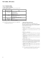
Page 82: ...nt detection of theY drive reset circuit 3 PD due to the over voltage detection of theY drive D D converter output VH150V 4 PD due to the over current detection of the Y drive D D converter output VH150V POWER SUPPLY MODULE 1 PD due to the over current detection of the large power supply VSUS 175V VOFS 150V VCSP 40V VRN 190V VADR 30V 2 PD due to the over voltage detection of the large power supply...

Page 83: ...ontrol signal fault Control signal stuck VH over current mode Scan IC mis operations Scan IC fault Scan IC control signal fault VSUS 175V line fault When small signal block power overload Fault of small signal block power supply of assemblies Fault of only the POWER SUPPLY MOD When not small signal block power overload Fault of the POWER SUPPLY MOD when PD occurs in the POWER SUPPLY MOD alone Faul...

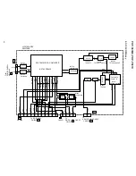
Page 84: ...IC2610 Q2702 IC2611 K2609 D2604 D2703 K2611 X DRIVE A B ASS Y E IC3101 Q3201 Q3204 D3322 CN3305 D3320 D3104 K3109 D3209 IC3106 Y DRIVE A ASS Y G IC3101 IC3106 Q3201 Q3204 D3209 D3324 D3104 K3109 D3310 CN3305 Y DRIVE B ASS Y H ...

Page 85: ...REG REG VSUS D2703 D2604 VCP F12 G9 PDF PDXA PDXB P12 VSUS PSUS XA Q2708 XPR V CPU IC3703 PD5438A M38067 E12 CN3702 E19 76 78 TEMP1 TEMP2 VCP O C Same as XA PD XA P4 PD XB Power Down Circuit BLOCK DIAGRAM 3 2 8 POWER SUPPLY MODULE X DRIVE A ASSY X DRIVE B ASSY Y DRIVE A ASSY Y DRIVE B ASSY PDYA PDYB µ COM ASSY 8 5 7 8 10 10 9 8 10 8 10 F10 Q3103 VCP 12V Q3215 P SUS_B Q3204 Q3101 CN3103 CN3102 D310...

Page 86: ... PRO TECTION IC3101 PULSE MODULE IC PULSE GEN IC3106 PULSE MODULE IC PULSE GEN IC3109 DRIVE PROTECTION IC3101 PULSE MODULE IC PULSE GEN IC3106 PULSE MODULE IC PULSE GEN IC3109 DRIVE PRO TECTION AWV1728 DIGITAL VIDEO ASSY DIGITAL SIGNAL PROCESS IC1271 OSD IC IC1242 PLL IC IC1551 SEQUENCE CONTROL IC IC1131 1151 1171 AD CONVERTER IC1301 PICTUER CONVERT IC IC1351 GRADATION PROCESS IC1401 1451 1501 MEM...

Page 87: ...62GS Y C SEP YNR IC3204 UPD6487GF3BA CLOCK GEN IC3352 UPC1861GR Field Buffer2M IC3202 MN4777AS 3D Y C SEP ASSY AWZ6332 IC3205 MN4776AS IC3355 MC14577CP IC3353 NJM2234M 3D C V S SW SCL To IC3204 SDA 3D Y VR3351 C LEVEL ADJ Field Buffer1M IC3201 UPC659AGS 4 3 5 34 22 6 97 96 100 86 85 81 56 SCL SDA 57 20 23 11 10 16 36 4 16 7 94 5 3 7 3 1 7 1 2 3 88 1 1 3 To ANALOG VIDEO ASSY CN4102 W17 VR3350 FREE ...

Page 88: ...5 Y Y G Y B Y R Y Pb Pr C 3 7 1 3 7 3 7 2 12 17 1 15 4 6 2 1 3 6IPQ_Y IPQ_BY IPQ_RY 12 13 5 14 7 9 10 12 9 11 13 4 15 3 2 1 4 2 4 4 2 2 3 5 20 22 23 14 3 5 13 12 14 15 10 9 S_OX SCAN CN9501 V_S V_SW2 1 3 5 1 7 1 1 2 3 5 13 5 4 3 7 5 3 1 12 14 4 15 7 3 5 7 1 64 2 6 2 5 2 4 15 19 21 3 V IN V IN S IN Y G CB B CR R BNC BNC RCA V OUT ANALOG VIDEO ASSY AWZ6305 K4501 V Y STD BY STD RY VD B Yout DU DV R Y...

Page 89: ...501 W1 RGB ASSY AWV1687 EEPROM SDA VD B B VD HD G G R R HD RGB2 IN RGB2 OUT Y G Pb B Pr R HD CB VD RGB1 SCL IC5805 M62358FP IC5311 TC74VHC123AFT 5 18 28 16 17 6 12Ch D A V_SW1 CLP2 47 IPQV 49 IPQH 26 30 SHARP NESS 32 RGBSW2 36 Y G 3 Y_SYNC 1 Pr R 7 Pb B 5 B Y Y R Y B SDA SCL CLP K6020 K6024 K6025 HBLK VBLK VDP G R B 7 PLL_HD PICTURE CONTROL V_MUTE CLP G R 9 11 13 24 SCL SDA S2_DET CLAMP COMPA RATO...

Page 90: ...AM CONTROL RAM CONTROL RAM CONTROL 20 3 3V CN1001 CONNECTOR for PANEL U COM to PANEL U COM To X DRIVER ASSY To RGB ASSY K1101 K1111 K1121 VRB VRT VRB VRT VRB VRT K1172 K1171 K1152 K1151 K1122 K1112 K1102 K1131 K1132 VCKB K1173 PLL BLOCK K1250 ADCK K1249 ADCK K1247 RST K1248 RST K1253 K1242 K1201 PD_EN SER OUT PLL_ULK K1261 VCLK2 K1262 HD1 K1263 VD1 K1264 FLD1 SYNC PROCESSOR PDY038B To POWER SUPPLY...

Page 91: ...PANEL X ELECTRODES IC2604 REG IC2603 REG IC2601 IC2602 IC2606 IC2607 3 4 5 6 9 13 14 15 20 21 22 VDD2 VSS2 SUSD VDD3 SUSG VSS3 4 1 2 1 2 33 VFX VFX 31 29 27 25 23 XPR U MUTE XSUS B XSUS D XSUS U XSUS G SUSB U D G RP U MUTE For Drive B PSUS PANEL X ELECTRODES G7 G6 G5 From Power Supply ASSY P12 To X Drive B ASSY G9 X DRIVE B ASSY has exactly same circuit as X DRIVE A ASSY From DIGITAL VIDEO ASSY D8...

Page 92: ..._A IC3310 VH_B GNDH_B IC5V_B H7 H8 IC3113 IC3112 IC3111 IC3110 IC3017 IC3015 IC3013 IC3018 IC3016 IC3014 IC3205 IC3206 Q3201 Q3205 Q3204 Q3207 Q3206 Q3208 Q3209 VOFS SUSOUT CSP Q3103 Q3101 H2 H3 H2 H6 H9 H11 H12 H10 CP BYPASS CLK_A LE_A SI_A STB_A TSC VH_A GNDH_A 29 25 23 21 19 17 15 11 1 IC5V_A 5 CP BYPASS CLK_B LE_B SI_B STB_B TSC VH_B GNDH_B 29 25 23 21 19 17 15 11 1 IC5V_B 5 8 CLK_A 11 SI_A 13...

Page 93: ... H 500µsec 0V YNR_D YNR_U D GND YNR_ D YNR_ U 0V 0V V 2v div H 500µsec PSUS_B SUS GND V 50v div H 500µsec SEL_HA SEL_LA D GND V 2v div H 500µsec 0V XSUS_G U B D D GND V 5v div H 1µsec 150µsec 150µsec XSUS_ G XSUS_ U XSUS_ B XSUS_ D SEL_HA SEL_LA 0V 0V 0V 0V 0V 150µsec 7µsec 1 3 5 6 4 2 ...

Page 94: ... 6 1 21 5 9 19 49 47 33 21 19 11 9 5 3 2 3 10 13 20 21 SDA HD2 VD2 CLK2 DATA2 SCL 6 5 2 18 3 2048fH 1024fH 6 5 18 14 13 22 19 4 10 10 14 10 K3703 66 4 5 SYSTEM MICRO COMPUTER U COM ASSY AWV1689 IC3703 PD5435 K3709 K3706 K3707 K3711 K3712 K3710 EEPROM PLL IC FULL AUTO ZOOM IC A D 8bit 1 2 1 1024 IC3704 24LC64 I SN IC3906 TC74HC02AF IC6441 TA8667F IC6471 HG62G010R29FB IC6431 TC35071 IC6481 TC74ACT74...

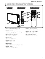
Page 95: ...f display Turns the display s power ON OFF 4 Power button Turns the power ON OFF Standby 5 INPUT selection button Used to select input 6 MENU button Used to switch between menu screens and the regular picture 7 ADJUST button Used to adjust various settings on the unit Main unit Operation panel Remote control unit 1 2 3 4 5 6 7 8 9 10 8 PANEL FACILITIES AND SPECIFICATIONS 8 DISPLAY Display call but...

Page 96: ...ut HD CS VD TTL level 2 2 kΩ input Compatible input signal Component video signal RGB signal G ON SYNC compatible Refer to next page for input compatible frequency With output jack Mini D Sub 15 pin 75 Ω output Note 4 Compatible with Microsoft s Plug Play VESA DDC1 2B Accessories AC Power cord 1 BNC conversion connector 3 Remote control unit 1 AA R6 UM 3 batteries 2 Cleaning cloth 1 Speed clamp 2 ...

Reviews: