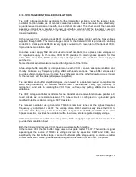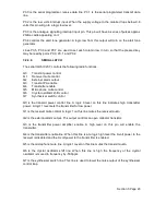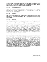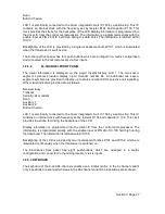
the display, whilst the 64-channel variant utilises both back planes and thus requires two
groups of data. Note the period of the serial clock when addressing the display driver is
approx 10 times greater than that required for the other serial devices.
3.2.4.7.3
CTCSS encoder/decoder
The CTCSS encoder/decoder is programmed in the period following the synthesizer
programming while waiting for the synthesizer loop to lock. It is programmed by first clocking
out 8 bits of serial data using the clock and data lines. Next a load pulse is applied to the
device and the new data is latched in.
3.2.4.7.4
Serial Latch
The serial latch is programmed by first clocking out 8 bits of serial data using the clock and
data lines. Next a load pulse is applied to the device, the serial data is latched in and the
outputs change.
3.2.4.7.5
Synthesizer
The synthesizer on the radio pcb is serially programmed by the main control processor. The
clock, data and enable signals are provided from ports PLO, P1.1 and P1.3 of IC206. These
logic control signals are directed via D207, D208 and D206 which prevent noise from the
micro processor being coupled to the RF synthesizer. When the synthesizer is being
programmed by the control processor the enable line is set to a logic high level. Then a series
of 29 clock pulses along with 29 bits of data are serially clocked into the synthesizer IC. Finally
the enable line is returned to the logic low level. The clock pulses will typically be of luSec
duration. Some pulses may appear to be stretched but this is due to the operation of the
control processor, and is normal. The rate at which the synthesizer is reprogrammed is
dependent on the mode of operation of the mobile. If the synthesizer is out-of-lock then the
control processor will attempt to reprogram the synthesizer approximately every 40mSec.
Whereas if the mobile is scanning with CTCSS selected it may be as long as 400mSec
between successive reprogramming of the synthesizer.
3.2.4.8 SELECTIVE CALL SIGNALLING
The selective call signalling in the PRM80 is achieved by means of a software control program
operating in the main control micro processor for both encode and decode functions. During
decode operation the pre-emphasised receive audio from the receiver is filtered by the
bandpass filter consisting of IC205a. This filtered audio is then passed to the zero-crossing
detector consisting of IC205b, IC205c, TR207, TR208, C249, C250, R261 and R262. During
positive signal input the output of IC205 goes logic high. This logic high is then coupled via
C250 to the base of transistor TR208 turning it on for a period of approx 20uSec. Resistor
R262 ensures that TR208 turns off and also effects the length of the pulse. The collector of
TR208 then pulls down resistor R260 to logic 0 level for this short period. For negative signal
input the same process occurs with IC205c, C249, TR207 and R261. Thus there is a logic 0
pulse for every zero crossing of the input signal. The series of pulses produced is applied to
the interrupt pin of the main control processor, IC206 for processing.
Section 3 Page 25


