background image

Serial Number

200001

Hardware 12NC

9525 001 10072

Application Code
Frequency Band

470 - 500MHz

Encode Signalling
Options
Encode Type

Identity

Tone Period

Individual Identity (1)

53454

l00ms

Individual Identity (2)

45554

l00ms

Individual Identity (3)

45453

l00ms

Emergency Identity

45345

l00ms

Emergency Identity

45435

looms

Individual Call

45345

looms

Encode Tone Set

CML CCIR

Lead in Delay

mSec

600

Lead out Delay

msec

100

Decode Signalling
Options
Indiv Decode Identity

45345

Group Decode

435345

Reset Decode Identity

43534534

Decode Tone Period

l00ms

Decode Tone Set

CIVIL CCIR

Scan Group Selection

Is Selectable Priority

Required

No

Priority Channel

3

Channels in Scan

14679

Channel Table

Rx

TX

Ch

Freq

Lock

CTCSS

Freq

Lock

CTC/ Selc Co

Scan Power

1

471.0000

No

471.0000

No

Yes

No

Yes

High

3

475.0000

No

No

No

Yes

High

4

476.0000

Yes

No

No

Yes

High

5

477.0000

No

478.0000

Yes

Yes

No

No

High

7

480.0000

No

481.0000

No

No

No

Yes

High

9

495.0000

No

No

Yes Yes

High

1.5.9

Equipment Data Sheet

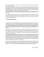
An individual data sheet listing all transmitter and receiver frequencies, including
signalling information, is supplied with each transceiver. It is important that this data
sheet is retained for future use such as the equipment requiring repair or change to
parameters (eg. channels or identities). A sample data sheet is shown below.

Section 1 Page 16

Summary of Contents for PRM80 Series

Page 1: ...ovember 1989 This handbook Is for the maintenance of telecommunication equipment The performance figures quoted are typical and are subject to normal manufacturing and service tolerances The right Is reserved to alter the equipment or specifications In the light of technical development This publication Is copyright and no part may be reproduced or copied without the prior permission of Philips Ra...

Page 2: ... Selective Call Facilities 13 1 5 8 Alert Tones 15 1 5 9 Equipment Data Sheet 16 SECTION 2 TECHNICAL SPECIFICATIONS Section 2 Page 1 2 1 GENERAL 1 2 2 RECEIVER 3 2 3 TRANSMITTER 4 2 4 SIGNALLING 5 2 4 1 PRM80 Selcall Specification 5 2 4 2 PRM80 CTCSS Specification 7 SECTION 3 TECHNICAL DESCRIPTION Section 3 Page 1 3 1 GENERAL OVERVIEW 1 3 1 1 Receiver 2 3 1 2 Transmitter 2 3 1 3 Synthesizer 3 3 1 ...

Page 3: ...ge 1 5 1 GENERAL INFORMATION 1 5 1 1 Operator Access 1 5 1 2 Location Dangers 1 5 1 3 Vehicles Fitted With Electronic Devices 1 5 1 4 Specialised Vehicles 2 5 1 5 Dash Mounted Equipment 2 5 1 6 Petrol Powered Vehicles 2 5 1 7 Gas Powered Vehicles 2 5 2 MAIN UNIT FITMENT 3 5 2 1 Cradle Installation 3 5 2 2 Transceiver Fitment 3 5 2 3 Transceiver Removal 3 5 2 4 Microphone Installation 3 5 2 5 Micro...

Page 4: ... design provides full band coverage without the need for mechanical tuning Similarly a range of broadband transmitter power amplifiers offering a selection of power output levels provide full band coverage without the need to mechanically re tune The local control front panel is available in two versions One version provides up to 9 channels and control of a limited set of software programmable op...

Page 5: ...O 10 ppm 30 to 60 Deg C Extended temp option vi Receiver Mute Adjustable Preset Additional components required on printed circuit board vii Signalling Without CTCSS encoder decoder With CTCSS encoder decoder Additional components on printed circuit board Standard Selcall High performance Selcall Additional components on printed circuit board viii Systems Standard no systems interface Systems inter...

Page 6: ...he front panel PCB is via a flexible printed circuit with a zero insertion force socket fitted to the front panel PCB No wiring looms are used in the mechanical assembly A moulded plastic sleeve provides a styling cover over the PCB and chassis assembly The front panel PCB is housed in a separate plastic moulding In the 9 channel front panel four moulded plastic buttons are clipped in as part of t...

Page 7: ...erconnection At this level of assembly the equipment may be operated and aligned Access to the component side of the control PCB is possible The majority of the components on this board are surface mounted and may be serviced with the PCB in situ To gain access to the radio PCB the radio screen must be detached nine fixing screws The equipment may be operated at this level of assembly but with deg...

Page 8: ...nsmitter power amplifier devices have the correct amount of heatsink compound applied to their mounting faces before fixing to the chassis Should the interconnecting flexible printed circuit fail a hand solderable replacement alternative is available The factory fitted flex strip must first be carefully removed from the control PCB by applying a hot air de soldering tool to the solder joint and pe...

Page 9: ......

Page 10: ...kit Not require d Not require d Not fitted Philips Stand ard conne Not fitted Variab le 7 S 12 5 5pp m T0 1 to 25 Std Local PRM8 010 ENC Selcall ENC Swivel bracke t Stand ard Stand ard Fitted None fitted Bypas sed for Fitted I Fixed 2 R 20 E0 68 88 2 5p p 1 to 25 PRM6 020 ENC DEC Selcall ENC Stick Comp act 3 V 25 80 132 I56 1opp m T0 to T T0 6 Low ENC DEC plus DTMF 4 X 30 A9 1445 T74 2 5pp m 30 to...

Page 11: ......

Page 12: ...ccurs TURN OFF Your Mobile Radio IMMEDIATELY and contact your Sales Representative for advice 5 Fans power accessories window demisters or radios may alter the operation of your mobile radio Consult the accessory manufacturer for details regarding the elimination of radio interference from such accessories 1 5 2 Advice to User 1 Only transmit when the channel is free 2 Do not speak while you can h...

Page 13: ...cribed in section 1 5 5 Scanning functions are described in section 1 5 6 Selcall functions are described in section 1 5 7 Some specially adapted application packages may include facilities described separately in supplementary information sheets 1 5 4 Common Functions And Facilities 1 5 4 1 SWITCH ON OFF To switch on press the On Off switch The LCD Liquid Crystal Display backlighting will be on w...

Page 14: ...ect operating procedure and keep transmissions short Release press to talk switch as soon as the message is finished and note that the transmit indicator is turned OFF When the transmit limit timer option is fitted the transmitter will be turned off at the end of preset time and a warning signal if programmed will be heard until the press to talk switch is released Re pressing the press to talk sw...

Page 15: ... usually programmed together and only on carefully controlled closed radio systems On such systems users are prevented from listening to the channel 1 5 5 5 CTCSS CONTINUOUS TONE CONTROLLED SQUELCH SYSTEM When CTCSS encode only is fitted a sub audio tone accompanies every mobile transmission If the CTCSS decode is supplied no communication will be heard unless the incoming transmission contains th...

Page 16: ... a valid signal until the microphone is removed from its cradle Scanning will only be active if the microphone is in its cradle ie on hook 1 5 6 1 OPERATION To enter Scan mode press the SCAN button The Scan chevron will turn ON The Channel display will be blanked and the SCAN indicator will start flashing If the error tones sound when the SCAN button is pressed it will mean that the scan group is ...

Page 17: ...lable are indicated below Please note that some of these may not be available on your equipment 1 5 7 1 SEND 1 The Send button causes a programmed identity to be transmitted This identity is used to identify the mobile to the base control 1 5 7 2 SEND 2 Used as Send 1 but provides for a second identity 1 5 7 3 ALARM Alarm is a special version of Send It is used to indicate the presence of an alarm...

Page 18: ... identity to acknowledge that a call has been received This switch is used to enable disable this facility 1 5 7 8 SELCALL RECEPTION Whenever a valid call is received the equipment will display the Call indicator It will also sound the appropriate call alert You may answer the call by operating the press to talk switch The indicator and alert tone will be cancelled Additionally if programmed remov...

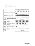
Page 19: ...Y Generated when any button Is BEEP pressed TONE 4 DECODE 1 Generated for selcall decode ALERT response TONE 5 URGENT Generated for selcall urgent ALERT response TONE 6 GROUP Generated for selcall group ALERT response TONE NORMAL Generated for selcall normal DECODE response ALERT TONE 1 5 8 Alert Tones The frequency of all alert tones is 500Hz Section 1 Page 15 ...

Page 20: ...VIL CCIR Scan Group Selection Is Selectable Priority Required No Priority Channel 3 Channels in Scan 14679 Channel Table Rx TX Ch Freq Lock CTCSS Freq Lock CTC Selc Co Scan Power 1 471 0000 No 471 0000 No Yes No Yes High 3 475 0000 No No No Yes High 4 476 0000 Yes No No Yes High 5 477 0000 No 478 0000 Yes Yes No No High 7 480 0000 No 481 0000 No No No Yes High 9 495 0000 No No Yes Yes High 1 5 9 E...

Page 21: ...88 MHz Tm 400 440 MHz B0 132 156 MHz U0 440 470 MHz A9 146 174 MHz W 1 470 500 MHz W4 500 520 MHz Channel Spacing VHF UHF 12 5 kHz 12 5 kHz 20 kHz 20 kHz 25 30 kHz 25 kHz Frequency Stability UHF VHF option 5ppm 10 Deg C to 60 Deg C better quality crystal VHF 10ppm 10 Deg C to 60 Deg C standard crystal VHF UHF USA 5ppm 30 Deg C to 60 Deg C extended temp option UHF 2 5ppm 10 Deg C to 60 Deg C TCXO U...

Page 22: ...5 5A less than 6 5A Type Approval Compliance The PMR80 is designed to comply with the following regulatory specification standards i Australian DOC RB206 RB207 RB234B ii New Zealand RTA25 III Canada RS119 iv European CEPT TR24 01 Annex 1 2 5 7 MPT 1306 MPT 1316 MPT 1326 v EIA RS 15213 RS204C Does not comply with squelch sensitivity 17 0 or Temp range 22 0 vi FTZ A446 82023 AA446 82024 Dimensions L...

Page 23: ... 85dB with a single signal ii UHF Greater than 80dB with a single signal Blocking Greater than 93dB ratio at 150kHz offset 2 generator method Modulation Acceptance Bandwidth i 12 5 kHz channel spacing greater than 4kHz ii 20 kHz channel spacing greater than 7 0kHz iii 25 30kHz channel spacing greater than 8 5kHz Spurious Radiation 9kHz to 1GHz less than 2 nW 1GHz to 4GHz less than 20 nW AF Regulat...

Page 24: ...at 20dB SINAD Response for 1 uV RF level less than 40mSec Mute Range Channel Spacing 12 5kHz 25kHz maximum 18 to 20dB 20 to 25dB SINAD Minimum l0dB l0dB SINAD 2 3 TRANSMITTER Power Output Adjustable 1 to 6 watt 1 to 25 watt 10 to 40 watt Spurious Emission Less than 0 25uW 100kHz to 1GHz less than 1uW 1GHz to 4GHz Residual Hum and Noise Greater than 40dB Reference 1 kHz at 60 deviation DC to 25kHz ...

Page 25: ...et to 80 or system deviation adjustment range typically 33 to over 100 of system deviation ii Tone Distortion Not greater than 10 at TX VCO input iii Tone Frequency Range 63 possible tones in the range 459Hz to 2937Hz See Table 2 2 for details iv Tone Amplitude Variation Not greater than 6dB over 459Hz to 2937Hz v Tone Frequency Error Not greater than 1 0 30C to 60C vi Tone Period 14 possible dura...

Page 26: ...e success rate sinad is measured at speaker output 1 Standard Selcall 20mSec 14dB Sinad 40mSec 15dB Sinad l00msec 13dB Sinad 255mSec l4dB Sinad 2 Enhanced Selcall 20mSec TBA 40mSec TBA 100mSec TBA 255mSec TBA ii Deviation Sensitivity Minimum deviation for 90 success rate and full receiver quieting 1 Standard selcall Less than 0 3kHz deviation 2 Enhanced selcall TBA iii Decode Bandwidth 80 deviatio...

Page 27: ...Less than 5 0 iii Frequency Accuracy 0 30 over 30 degC to 60 degC iv Number of Tones There are including disabled 38 available tones See Table 2 1 2 4 2 2 Reverse Tone Burst In order to prevent the mute tail associated with the de response time of CTCSS decoders the mobile may be equipped with reverse tone burst RTB This RTB occurs at the end of CTCSS transmission and consists of a period of CTCSS...

Page 28: ...eviation at 1kHz v False Decode Rate Less than 5 false decodes per minute no carrier input vi Talkoff I nterfering tone deviation for loss of decode CTCSS tone deviation 10 of system Full quieting RF signal 310Hz to 3kHz 90 of system deviation for no dropouts 20dB sinad RF signal 320Hz to 3kHz 90 of system deviation for no dropouts in one minute 12dB sinad RF signal 350Hz to 3kHz 90 of system devi...

Page 29: ...7 3 Hz 131 8 Hz 136 5 Hz 141 3 Hz 146 2 Hz 151 4 Hz 156 7 Hz 162 2 Hz 167 9 Hz 173 8 Hz 179 9 Hz 186 2 Hz 192 8 Hz 203 5 Hz 210 7 Hz 218 1 Hz 225 7 Hz 233 6 Hz 241 8 Hz 250 3 Hz 00 17 18 19 20 21 09 22 01 23 10 38 02 11 03 12 04 13 05 14 06 15 07 16 08 24 25 26 27 28 29 30 31 32 33 34 35 36 37 150 140 140 140 130 130 130 130 120 120 120 120 120 110 110 110 110 110 110 110 110 110 110 110 110 90 90...

Page 30: ...70 2247 2400 2110 2400 1060 1160 1270 1400 1530 1670 1830 2000 2200 2800 810 970 886 2600 2400 1060 1160 1270 1400 1530 1670 1830 2000 2200 970 2800 2600 2400 1060 1160 1270 1400 1530 1870 11830 2000 2200 2900 2800 741 970 810 886 2400 1060 1160 1270 1400 1530 1670 1830 2000 2200 2800 970 885 2600 2400 1080 1160 1270 1400 1530 1670 1830 2000 2200 970 885 741 2600 2800 600 2400 1060 1160 1270 1400 ...

Page 31: ...ircuit board assemblies i Front Panel Board Containing the liquid crystal display its driving circuit push button switches and display backlighting ii Control Board Containing the microprocessor with its associated clock and latches EEPROM memory power supply and reset circuit transmitter audio processing receiver audio processing selective call audio processing and CTCSS signalling option Section...

Page 32: ...red to remove residual 455kHz products and then further audio frequency processing such as 300Hz to 3000Hz band pass filter and de emphasis is provided The mute gate is placed before the volume control adjustment which is ahead of the audio power amplifier The demodulated output is also high pass filtered amplified and detected The quieting of the detected noise provides for mute control 3 1 2 Tra...

Page 33: ...e In addition to this other major functions include programming of the synthesizer controlling the display of LCD information controlling the receiver audio mute and transmit microphone mute monitoring the front panel buttons controlling CTCSS and reverse tone burst signalling and performing the task of programming and reading the electrically erasable memory The electrically erasable memory conta...

Page 34: ...microprocessor This maintains stored information during short duration power failures and also retains the last programmed state when the transceiver is switched off To ensure reliable operation of the microprocessor an interrupt and reset circuit is provided This circuit detects power failure and induces the microprocessor to prepare for a reset The timing between interrupt and reset is carefully...

Page 35: ...he synthesizer via resistors R401 and R403 The remainder of the front end consists of a low noise transistor preamplifier in TR400 followed by a tuned bandpass filter using three coupled resonators X402 X403 and X404 This three section filter operates in a similar manner to the first pair already described Conversion to the first IF frequency of 21 4MHz is achieved with the double balanced ring di...

Page 36: ...ic filter FL404 This filter provides the final stage of adjacent channel rejection and it s performance in conjunction with FL403 provides the overall selectivity of better than 75dB FL403 also has sufficient selectivity to reject the second image at 910kHz offset The IF signal at the output of the second mixer PIN 3 is processed externally to IC400 by the noise blanker option when this module is ...

Page 37: ...is frequency band is effectively out of band demodulated noise The amplified noise is half wave rectified at the output of IC401 PIN 14 by diode D426 which is forward biased The integrator capacitor loading the rectifier is C466 The rectifier configuration actually provides a voltage doubling in the charging of C466 The third stage of OP AMP IC401 is configured in a Schmitt trigger circuit which c...

Page 38: ...ifier is shown in block diagram form in figure 3 4 The amplification is achieved in four discrete stages The first stage has an input of 20mW from the transmit VCO This becomes amplified by TR417 operating in class AB mode to a level of approximately 200mW Diode D443 provides temperature stability of the bias for this amplifier stage The next stage of amplification occurs in TR419 which produces u...

Page 39: ...couples the output power to the antenna socket The bias current for D439 flows into D440 and D441 via a PI section equivalent quarter wave transmission line Transistor TR428 is also biassed on and provides the ground return for diodes D440 and D441 Diodes D440 and D441 are biassed on and form a short circuit across the receiver input to achieve isolation from the transmitter This short circuit is ...

Page 40: ...and will thereby reduce the transmitter output power providing a further measure of protection A second potentiometer R578 is used to reduce the reference voltage when low power operation is selected The output from the power amplifier is coupled to the antenna socket via a solid state antenna changeover circuit and harmonic filter In the receive mode D439 D440 and D441 are all reverse biased The ...

Page 41: ...meter The output of the microphone amplifier stage may pass directly to the following stage which is a clipper circuit Alternatively the signal may pass via the CTCSS high pass filter which has the input at PIN 22 of IC204 and output at PIN 20 When CTCSS is fitted IC204 provides additional rejection of low frequency microphone audio below 300Hz to ensure a minimum disturbance of the CTCSS encode t...

Page 42: ...ion of the transmitter power amplifier It is very important to obtain a low single side band phase noise for both of these signal sources to achieve the required levels of receiver and transmitter performance These objectives have been achieved by utilizing a single phase locked loop with a high gain phase comparator and independent receive and transmit low noise VCOs 3 2 3 2 THE BASIC PHASE LOCKE...

Page 43: ...two buffer amplifier stages The output of each VCO is combined in a passive resistor combining network and a buffer amplifier is provided ahead of the synthesizer frequency divider chain The frequency dividers consist of a dual modulus divide by 64 or 65 prescaler device Plessey SP8718 followed by the programmable divider IC Plessey NJ8822 In this integrated circuit are two programmable dividers o...

Page 44: ...oximately 5uSec The entire data stream occurs in a burst of approximately 150uSec duration When the loop is out of lock the re programming occurs every 40mSec During the burst of data the chip enable input at PIN 14 is held high The high gain sample and hold phase comparator has adjustable gain which is set by an external resistor R518 at PIN 17 and capacitor C522 at PIN 15 These components are op...

Page 45: ... in a modified Pierce oscillator circuit using a quartz crystal XL401 in the feedback path Feedback occurs between the base and collector of TR413 which provides 180 degree phase shift The crystal operates in a parallel resonance mode to provide a further 180 degree phase shift The oscillator is tuned to the correct frequency of 10MHz by a tunable coil L411 placed in series with the crystal Varica...

Page 46: ...cient output power to drive the synthesizer and the other following circuits mixer for the receiver and the transmitter power amplifier The oscillator and buffer amplifier stages are housed in separate screened compartments which are provided by the die cast radio screen This ensures a very high immunity to microphony and aids in isolating the VCO from the frequency pulling effects due to load var...

Page 47: ... program synthesizer change display information etc To effect control via the serial bus the integrated circuit under control is enabled during the period of the data burst All the operational characteristics of the software are fixed in the masked program memory within the microprocessor The external EEPROM is required to provide the microprocessor with information on which software options are t...

Page 48: ...eceiver supply is disabled To activate the transmitter power amplifier the microprocessor provides a separate control output PA enable via the latch IC207 at PIN 7 to enable transistor TR217 When TR217 is enabled TR216 is biased on and supplies the transmitter buffer stage TR417 with power A timing delay of 40mSec is provided between 9V Tx and 9V PA output to ensure the synthesizer frequency has s...

Page 49: ...m application of the 9V supply A high current 9 volt supply for the LCD backlighting is provided by TR215 which obtains its bias voltage from TR214 In special systems applications it is necessary to provide the microprocessor with an indication of the power off status although the equipment is permanently powered on This is provided by the output of the voltage divider R365 R366 connected to PIN 2...

Page 50: ...t ports are configured to logic high Upon initial power application conditions may occur where the interupt becomes active low until the supply voltage has increased sufficiently to switch off TR224 In this case the RESET output must be held high TR233 is active during the initial power up and ensures that TR226 is biassed off and thereby TR227 conducts for the period of the time constant set by C...

Page 51: ...is input is active low ie a 0V level indicates microphone in cradle Line P0 4 comes from the microphone socket pin 4 via a suppression network consisting of C270 R282 and R278 This input is active low ie a 0V level indicates transmit and a high level 5V indicates receive Line P0 5 comes from the hardware mute detector circuit It is used to indicate to the control program the presence or not of an ...

Page 52: ...alarm input P2 1 RF power detect P2 2 Alarm power sense P2 3 3rd party option toggle P2 4 CTCSS encode RTB control P2 5 Analogue signalling control P2 6 Analogue signalling control P2 7 Analogue signalling control The external alarm input from SK203 pin 4 goes via R248 and bypass circuitry composed of C235 and D204 to P2 0 of the micro controller This pin is normally pulled up by R247 to a logic h...

Page 53: ...ne mute control Q6 Crystal oscillator shift control Q7 Synthesizer switch control Q0 is the transmit power control line A logic 0 level on this line indicates high transmitter power A logic 1 level sets the transmitter for low power Q1 is the receiver mute control A logic 1 on this line mutes the received audio Q2 is the external alarm output This output controls an open collector transistor Q3 is...

Page 54: ...a and command information While the device is internally programming the data out line serial data indicates the state of programming This data out line is low while programming and high when programming is completed This programming typically takes 5 to 10 mSec When all this is finished a write disable command of the same form as the write enable command is issued to the device Reading of the dat...

Page 55: ... pulses will typically be of luSec duration Some pulses may appear to be stretched but this is due to the operation of the control processor and is normal The rate at which the synthesizer is reprogrammed is dependent on the mode of operation of the mobile If the synthesizer is out of lock then the control processor will attempt to reprogram the synthesizer approximately every 40mSec Whereas if th...

Page 56: ...6 at a level of approximately 775mV rms The encode tone output has two alternate paths before being combined with the transmitter audio at PIN 13 of IC210 One path passes via C243 and the CMOS switch IC212 to the encode level setting potentiometer R354 The alternate path is via transistors TR230 and TR231 This circuit provides the 120 deg RTB feature The passive network of C241 C242 R344 and R345 ...

Page 57: ...o display up to status number 99 for selective call signalling Other visual indicators provided are as follows Receiver Busy Transmit Selcall call or called Scan Auxiliary 1 Auxiliary 2 Button Chevron LCD 1 is electrically connected to the driver integrated circuit IC 100 by a zebra strip This IC contains an internal clock with frequency set by resistor R 104 and capacitor C 100 This clock provide...

Page 58: ...is occurs for each of the three rows and the control program is then able to determine which key has been pressed and what action to take When a pressed key is detected it is debounced by reading the matrix a number of times to ensure that only one key press is registered Some keys have been designated as auto repeating keys in which case once the auto repeat sequence has been entered the matrix w...

Page 59: ...n insulated tool for all other adjustments where short circuits could occur iii The negative lead of all test equipment should be connected to the PRM80 chassis unless stated otherwise iv This alignment procedure assumes that the equipment is operating normally and is without faults 4 3 PRELIMINARY ADJUSTMENTS i Ensure test frequencies and options are programmed into the EEPROM This program is for...

Page 60: ... 525 25 4 132 025 132 525 1 107 2Hz 5 140 025 140 525 1 107 2Hz ENC test 6 155 025 155 525 1 107 2Hz A9 1 146 025 146 525 25 146 to 174 2 160 025 160 525 25 3 173 025 173 525 25 4 146 025 146 525 1 107 2Hz 5 160 025 160 525 1 107 2Hz ENC test 6 173 025 173 525 1 107 2Hz Tm 1 400 025 400 525 25 400 to 440 2 420 025 425 525 25 3 439 025 439 525 25 4 400 025 400 525 1 107 2Hz 5 420 025 420 525 1 107 ...

Page 61: ... 1 500 025 500 525 25 500 to 520 2 510 025 510 525 25 3 519 025 519 525 25 4 500 025 500 525 1 107 2Hz 5 510 025 510 525 1 107 2Hz 6 519 025 519 525 1 107 2Hz ENC test tone 4 4 1 Selcall Encode Test Program detail CML CCIR Lead in Delay 9999mSec Lead in Tone Required Lead in Tone 4 1358Hz Individual Encode Identity 1 1 2 3 4 5 40mSec Individual Decode Identity 1 2 3 4 5 40mSec Group Decode Respons...

Page 62: ... Step No Result Measured by Result Measured at Adjust Result Notes 1 Switch on power Select ch 3 Highest freq channel 2 Activate PTT 3 DVM dc volt range TP402 L445 15 0 0 2V 4 Disable PTT 5 DVM do volt range TP402 Select ch 1 and activate PTT 3 0 to 5 0V Lowest freq ch 6 Disable PTT Disconnect DVM 4 5 2 Transmitter Power Adjustment Step No Result Measured by Result Measured at Adjust Result Notes ...

Page 63: ...PTT 11 Transmit Power must be re adjusted when the radio screen is fitted See 4 5 7 step 10 4 5 3 Reference Oscillator Tuning Step No Result Measured by Result Measured at Adjust Result Notes 1 Switch on power Perform alignment 4 5 2 if not already completed 2 Select ch 2 Mid freq channel 3 Activate PTT 4 Frequency counter Via power meter at antenna socket SK402 L411 500Hz of correct frequency Che...

Page 64: ... div 10uSec per div 10x probe PIN 2 of U401 R557 Maximum level on CRC Typ 200mV p p Sets tracking gain adjustment 7 REPEAT STEPS 1 TO 6 TO ELIMINATE SLIGHT INTERACTION BETWEEN R554 AND R557 8 Select ch 3 Highest freq channel g RF sig gen output 1 mV pd level and freq of channel 3 10 AF level meter Speaker output at S K202 Volume control 300mW in 4ohm 11 AF level meter Speaker output at SK202 L404 ...

Page 65: ...q channel 6 RF sig gen output Freq of channel l 7 CRO 5mV per div l0uSec per div 10x probe PIN 2 of U401 R554 Max level on CRO Sets tracking offset adjustment 8 Select ch 3 Highest freq channel g Antenna socket SK402 RF sig gen output Freq of channel 3 10 CRO 5mV per div 10uSec per div 1 0x probe PIN 2 of U401 R557 Max level on CRO Slight re adjustment may be necessary 11 RF sig gen output 1 mV pd...

Page 66: ...2 RF sig gen output level a 23dB SINAD b 19 1dB SINAD a for 20 25 30 kHz channel spacing b for 12 5kHz channel spacing Record sig gen level 5 Switch off RF sig gen output 6 Speaker output SK202 Mute control fully clock wise AF should mute If AF does not mute adjust R455 7 Switch on RF sig gen Same output level as in step 4 Ensure AF is muted If AF does not mute adjust R455 slightly clockwise to ac...

Page 67: ...nna socket SK402 R316 a 4 8kHz 0 0 2 b 3 8kHz 0 0 2 c 2 4kHz 0 0 1 a 25 30 kHz channel spacing b 20kHz channel spacing c 12 5kHz channel spacing 6 Deviation monitor Antenna socket SK402 AF sig gen output freq 300Hz to 3kHz Output level 400 40mV rms Less than a 5 0kHz b 4 0kHz c 2 5kHz a 25 30kHz channel spacing b 20kHz channel spacing c 12 5kHz channel spacing 7 AF sig gen output 1 kHz freq 40 4mV...

Page 68: ... Adjust Result Notes 1 Perform Alignment Procedure 4 5 7 Leave Radio Screen Fitted When Test Is Completed Switch Off AF Signal Generator 2 Switch on power select channel 6 CTCSS test channel 3 Activate PTT 4 Deviation monitor Antenna socket SK402 R354 a 580Hz 30Hz b 460Hz 25Hz c 290kHz 15Hz a 25 30kHz channel spacing b 20kHz channel spacing c 12 5kHz channel spacing 5 Microphone socket SK201 AF si...

Page 69: ...ect channel 5 ch 6 UHF ch 5 VHF 3 LC Display Press SEND button Checks display 4 Deviation monitor Antenna socket SK402 R323 a 4kHz 200Hz b 3kHz 200Hz c 2kHz 100Hz a 25 30kHz channel spacing b 20kHz channel spacing c 12 5kHz channel spacing 5 Frequency counter at monitor Antenna socket SK402 1358 4Hz 6 The selcall test will cease after 10 Secs To i nterru pt the transmission the radio must be switc...

Page 70: ......

Page 71: ......

Page 72: ......

Page 73: ......

Page 74: ... of the transceiver 5 1 3 Vehicles Fitted With Electronic Devices An additional precaution is necessary in relation to vehicles fitted with Electronic Ignition Fuel Injection Anti skid Brakes or any other electronic device where temporary lass of service could be hazardous In theory any of the above systems could be affected by the presence of an RF field of sufficient intensity which when detecte...

Page 75: ...non reflective surface no protrusions or sharp corners Care must be taken when installing these to ensure that any additional metalwork necessary to fix the units into the vehicle conforms to the same requirement Refer to Section 5 2 for mounting cradle and transceiver fitment detail 5 1 6 Petrol Powered Vehicles Ensure that there are no petrol leaks before commencing an installation involving the...

Page 76: ... Two flat washers two spring washers and two screws are then fitted through the cradle into the sides of the transceiver Before finally securing these screws the transceiver may be tilted for optimum display viewability and access to the front panel controls 5 2 3 Transceiver Removal The removal procedure of the transceiver from the cradle is simply the reverse of the procedure specified in sectio...

Page 77: ... 1 to 2 Nm 8 85 to 17 7 lb ft ins Hexagon head version 2 to 2 5Nm 17 7 to 22 1 lb ft ins Cover retaining screw 3502 310 44180 when cradle is not used 1 to 2 Nm 8 85 to 17 7 lb ft ins All other retaining screws 1 to 2 Nm 8 85 to 17 7 lb ft ins 5 3 ANTENNA INSTALLATION For best all round performance of the radiotelephone the antenna should be mounted on the centre of the vehicle roof Alternative pos...

Page 78: ......

Page 79: ......

Reviews: