113
Chapter 4
Specifications
●
Output circuit diagram and terminal layout drawing
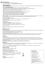
<SL-VTP□J>
200mA max.
T
r
Z
D
+24V
Power supply circuit
D
G
0V
+24V
Output
Load
S-LINK V
system side
0V
N.C.
Output device side
Main circuit
Internal circuit
Symbols… Z
D
: Surge absorption zener diode
T
r
: NPN output transistor
<SL-VTP□E>
200mA max.
T
r
Z
D
+24V
D
G
0V
+24V
Output
S-LINK V
system side
Output device side
0V
N.C.
Power supply circuit
Load
Main circuit
Internal circuit
Symbols… Z
D
: Surge absorption zener diode
T
r
: NPN output transistor
<SL-VTP□J>
0
Connector No.
+24V
0V
Output
N.C.
1 2 3 4
<SL-VTP□E>
+
24V
N.C.
Output
0V
1 2 3 4
Summary of Contents for S-LINK V
Page 2: ...2 ...
Page 5: ...5 Before Using This System ...
Page 12: ...12 Before Using This System MEMO ...
Page 13: ...13 Chapter 1 Designing System ...
Page 35: ...35 Chapter 2 Wiring ...
Page 60: ...60 Chapter 2 MEMO ...
Page 61: ...61 Chapter 3 Starting System ...
Page 71: ...71 Chapter 4 Specifications ...
Page 161: ...161 Chapter 5 Troubleshooting ...
Page 169: ...169 Appendix ...
Page 180: ...180 Appendix MEMO ...