APPENDIX A PROGRAM LIST
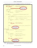
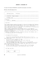
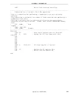
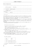
LSRCM = 0b00000001;
/* Stop the oscillation of the low-speed
internal oscillator */
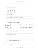
/* Initialize the port 2 */
P2 = 0b00000011;
/* Set output latches of P20, P21 as high
(turn off LED1, LED2) and P22, P23 as low */
PM2 = 0b11110000;
/* Set P20-P23 as output mode */
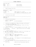
/* Check the reset source */
ucRESF = RESF;
/* Read the reset source */
if (ucRESF.4){
/* A reset generated by WDT */
P2 = 0b00000001;
/* Light LED2 */
}
if (!ucRESF.0){
/* Omit subsequent LVI-related processing during LVI
reset */
/* Set low-voltage detection */
LVIS = 0b00000111;
/* Set the low-voltage detection level
(VLVI) to 2.85 V +-0.15 V */
LVION = 1;
/* Enable the low-voltage detector operation */
for (ucCnt200us = 0; ucCnt200us < 9; ucC+){
/* Wait of
about 200 us */
NOP();
}
while (LVIF){
/* Wait for VDD >= VLVI */
WDTE = 0xAC;
/* Clear the watchdog timer */
}
LVIMD = 1;
/* Set so that an internal reset signal is
generated when VDD < VLVI */
}
/* Set the clock <2> */
PPCC = 0b00000001;
/* The clock supplied to the peripheral
hardware (fxp) = fx/2 (= 4 MHz) */
/* -> The clock supplied to the CPU (fcpu)
= fxp = 4 MHz */
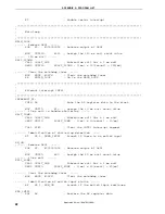
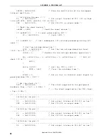
/*----------------------------------------------------------------------------
Initialize the port 0
----------------------------------------------------------------------------*/
P0 = 0b00000000;
/* Set output latches of P00-P03 as low */
PM0 = 0b11110000;
/* Set P00-P03 as output mode */
/*----------------------------------------------------------------------------
Initialize the port 3
----------------------------------------------------------------------------*/
P3 = 0b00000000;
/* Set output latches of P30-P33 as low */
PM3 = 0b11110000;
/* Set P30-P33 as output mode */
/*----------------------------------------------------------------------------
Initialize the port 4
----------------------------------------------------------------------------*/
P4 = 0b00000000;
/* Set output latches of P40-P47 as low */
Application Note U18847EJ1V0AN
32

