


RADIOBEACON TRANSMITTER
ND500II (125 WATTS) DOUBLE SIDEBAND - NO VOICE
Page 2-7
01 November 2003
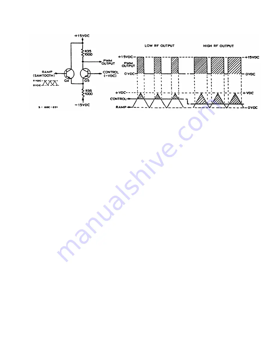
Figure 2-1 Simplified Schematic of PWM Differential Amplifier
2.2.4.9
Balanced Drive:
The balance drive circuit
is comprised of buffer amplifier U8C, transistors
Q6/Q7 and their associated components. The
balance drive forms a switching circuit that is driven
by the variable pulse-width modulation signal from
the variable pulse-width generator circuit. The pulse-
width modulated signal is inverted by buffer amplifier
U8C. Transistors Q6/Q7 will be gated on and off at
the PWM switching frequency. The switching action
of transistors Q6/Q7 ensures the leading and trailing
edges of the rectangular waveform are sharp. The
mod drive
output on connector J2-8 is a low
impedance pulse-width modulated signal switching
b15V and ground.
2.2.4.10
Pulse-Width Fault Detector
: The pulse-
width fault detector circuit is comprised of
operational amplifier U9B, inverter U8D, relay K1
and associated components. The subject circuit
monitors the pulse-width modulation signal for the
presence of +15 volt DC pulses. A two-pole low
pass filter network, comprising resistors R37/R38
and capacitors C21/C22, continuously monitors the
mod drive
output for the presence of positive voltage
pulses. When they are present, capacitor C21 will
charge to an average value, dependent on the on/off
ratio. The voltage on capacitor C22 that is applied to
the non-inverting input of U9B will not exceed the
reference threshold voltage applied to the non-
inverting input of U9B from the junction of resistors
R39/R40. The output of U9B will be low impedance
to ground, resulting in the output of U8D being
+15V. A
mod drive alarm
signal will not be applied
to J2-6.
If the voltage on capacitor C22 exceeds the reference
threshold voltage applied to the inverting input of
U9B, the output of U9B will be a +15V. Relay K1
will energize and remove the
mod drive
output on J2-
6. The output of U8D will be zero volts DC. A zero
potential
mod drive alarm
signal will be applied
through J2-6 to
MOD DRIVE ALARM
lamp DS3 on the
transmitter's front panel. The lamp will turn on.
2.2.5
POWER AMPLIFIER/MODULATOR
(A6)
(see figure SD-7): The power amplifier/
modulator is comprised of a modulator that provides
high level amplitude modulation of the carrier signal
plus an RF power amplifier. The RF power amplifier
provides 125 watts of carrier power at 100%
amplitude modulation over a frequency range of 190
to 650kHz and 100 watts of carrier power at 100%
amplitude modulation over a frequency range of 651
to 1250 kHz and 1600 to 1800 kHz.
2.2.5.1
Modulator
: The modulator circuit is
comprised of power MOSFET Q1 (connected as an
electronic switch) and associated components. Under
normal operating conditions, the
mod drive
input (J1,
zero to +15V pulses) is applied through inductor L3
to the gate of Q1. When the gate of Q1 is positive,
Q1 will be forward biased (turned on). Current will
flow through Q1, through a low-pass filter circuit,
formed by inductors L1/L2 and capacitors C1
through C5, to the B+ line. When the gate of Q1 is
negative, Q1 will be reverse biased (turned off). The
low-pass filter circuit removes the 70 kHz switching
frequency but passes the audio information.
Transistor Q1 will be switching on and off with a


