


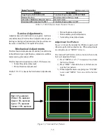


2-9
Lead Free Solder
Mitsubishi's 2005-2006 product line, including the V28,
V29, V30 and V31 chassis, will be constructed using
lead free solder.
This is the first part of a 3 phase program to eliminate
the lead content in all MDEA's electronic products. The
3 phases are:
• Phase 1… PCB's constructed using Pb-free
solder. PCB surface finishing and components
may contain Pb.
• Phase 2… Solder, PCB surface finishing and
component lead plating is Pb-free. Components
may have internal Pb.
• Phase 3… Solder, PCB surface finishing and
components are Pb-free. (100% Pb-free)
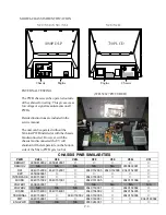
Pb-Free
Phase
Definition
Display
Short Display (W hen
the area is too small)
Phase-1
PCB's constructed using
Pb-free solder.
Phase-2
Solder, PCB surface
finishing and component
lead plating is Pb-free.
Components may have
internal Pb.
Phase-3
Solder, PCB surface
finishing and
components are Pb-free.
(100% Pb-free)
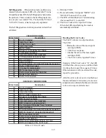
Table 2-1: Pb-Free Phases and Symbols
Pb PCA
Pb Joints
Pb S
Pb J
Pb P
Pb Solder
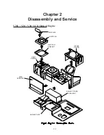
Displays used to indicate Pb-free
PCBs will be marked, indicating the level of Pb-free
construction.
Table 2-1
defines the levels by phase and
shows the different symbols that will be displayed on
the PCB. Additionally, a PCB constructed using Pb-
free solder may be simply marked
LFS
.
When possible, the indication will be placed close to
the part number that is screened onto the PCB (not the
part label).
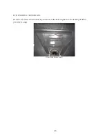
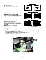
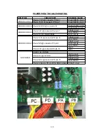
Figure 2-1
is an example of a PCB show-
ing the display and its location.
Pb free solder differs from conventional leaded solder.
• The amount of tin in Pb-free solder is greater.
• The melting point of Pb-free solder is higher.
Figure 2-1: Pb-Free Display on PCB
Pb-Free
Display
Summary of Contents for Mr.Slim WD-52627
Page 2: ......
Page 4: ...II...
Page 50: ...4 8...
Page 54: ...5 4 Figure 5 3A V28 PWB POWER DC to DC Supplies...
Page 55: ...5 5 Figure 5 3B DLP PWB POWER DC to DC Supplies...
Page 58: ...5 8 Figure 5 7 DLP Engine Power Supply Figure 5 8 Hard Disc HDD Power Supply V30 and V31 Only...
Page 59: ...5 9 Figure 5 9...
Page 60: ...5 10 Figure 5 10...
Page 63: ...5 13 Figure 5 13 Analog Video Signal Path...
Page 64: ...5 14 Figure 5 15 Video Record Path V30 and V31 only Figure 5 14 Analog Video Signal Path...
Page 69: ...5 19 Figure 5 22 DLP Engine Protect Circuitry Figure 5 23 Short Detection Circuitry...
Page 70: ...5 20...
Page 71: ......


