


DS3171/DS3172/DS3173/DS3174
191
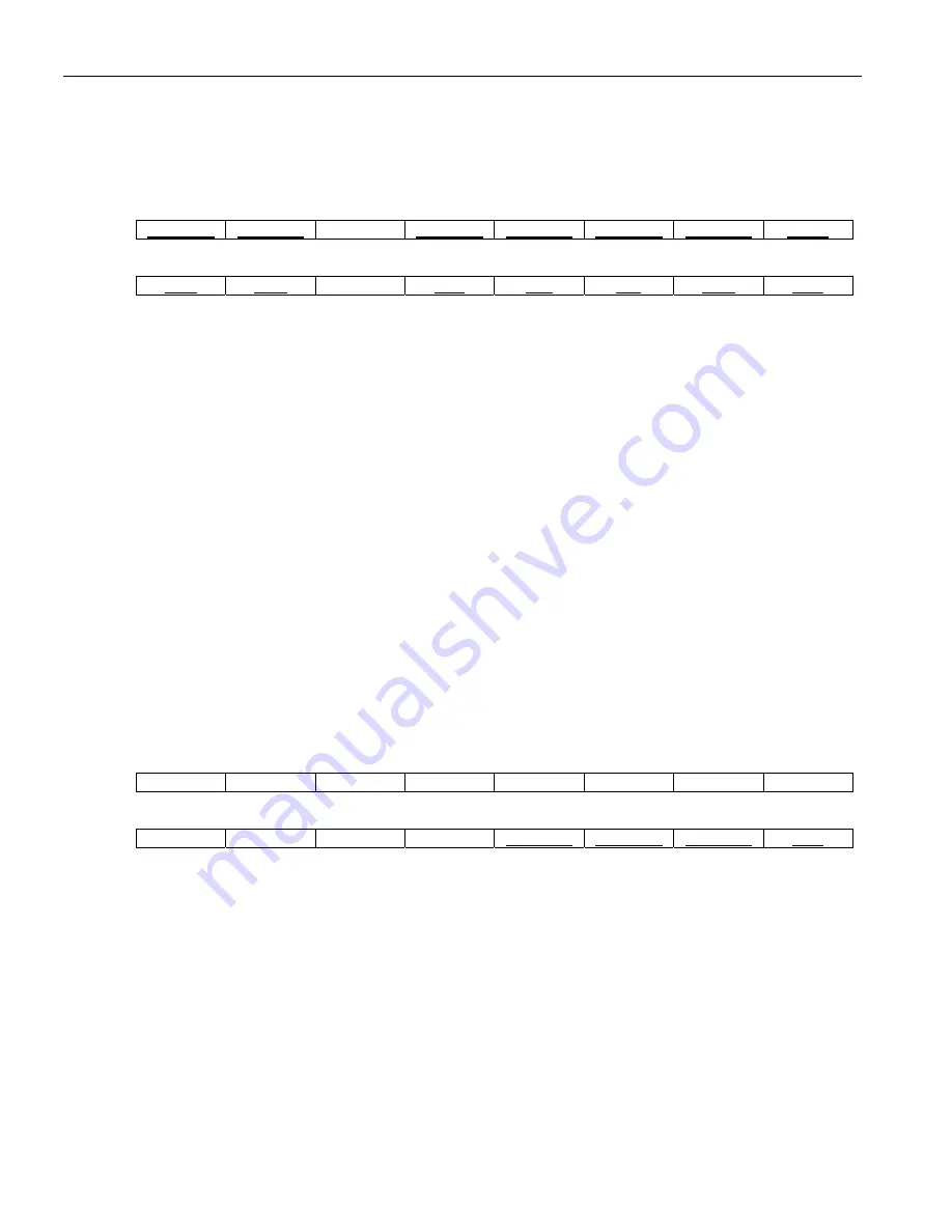
Register Name:
E3G751.RSR1
Register Description:
E3 G.751 Receive Status Register #1
Register Address:
(1,3,5,7)24h
Bit
# 15 14 13 12 11 10 9 8
Name Reserved Reserved -- Reserved Reserved Reserved Reserved RUA1
Bit
# 7 6 5 4 3 2 1 0
Name RAB RNB -- LOF RDI AIS OOF LOS
Bit 8: Receive Unframed All 1’s (RUA1)
– When 0, the receive frame processor is not in a receive unframed all
1’s (RUA1) condition. When 1, the receive frame processor is in an RUA1 condition.
Bit 7: Receive A Bit (RAB)
– This bit is the integrated A bit extracted from the E3 frame.
Bit 6: Receive N Bit (RNB)
– This bit is the integrated N bit extracted from the E3 frame.
Bit 4: Loss Of Frame (LOF)
– When 0, the receive frame processor is not in a loss of frame (LOF) condition.
When 1, the receive frame processor is in an LOF condition.
Bit 3: Remote Alarm Indication (RDI)
– This bit indicates the current state of the remote alarm indication (RDI).
Bit 2: Alarm Indication Signal (AIS)
– When 0, the receive frame processor is not in an alarm indication signal
(AIS) condition. When 1, the receive frame processor is in an AIS condition.
Bit 1: Out Of Frame
(OOF)
– When 0, the receive frame processor is not in an out of frame (OOF) condition.
When 1, the receive frame processor is in an OOF condition.
Bit 0: Loss Of Signal (LOS)
– When 0, the receive loss of signal (LOS) input (RLOS) is low. When 1, RLOS is
high.
Register Name:
E3G751.RSR2
Register Description:
E3 G.751 Receive Status Register #2
Register Address:
(1,3,5,7)26h
Bit
# 15 14 13 12 11 10 9 8
Name
-- -- -- -- -- -- -- --
Bit
# 7 6 5 4 3 2 1 0
Name
-- -- -- --
Reserved Reserved Reserved FEC
Bit 0: Framing Error Count (FEC)
– When 0, the framing error count is zero. When 1, the framing error count is
one or more.