4-40
Copyright © 2008 LG Electronics. Inc. All right reserved.
Only for training and service purposes
LGE Internal Use Only
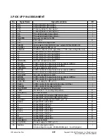
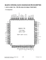
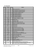
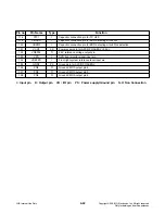
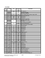
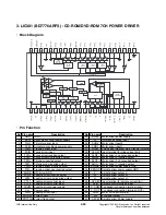
Pin no.
Pin Name
Type
Function
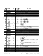
41
SH2
I
PCA peak/bottom detection, APC space detection/ Playback power
detection/Erase detection sample timing signal input pin (pulldown)
42
SH1
I
ROPC space detection, APC space detection/ Playback power detection
sample timing signal input pin(pulldown).
43
FEPIDGT/SH6
I
CAPA through signal input pin/servo sampling signal input pin (pull-down)
44
SH5
I
Sample-and-hold timing signal input pin of wobble S/H at recording (pull-down)
45
VCC4
PS
Power supply pin for internal LOGIC (5.0V)
46
LSDAT
I/O
Serial data input for LPC.
47
LSCK
I
Serial clock enable input LPC.
48
LSEN
I
Serial enable input for LPC.
49
TGCHG
I
LPC DAC bank change control signal input pin.
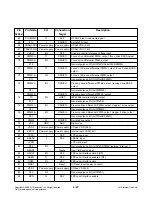
50
NC
-
-
51
CHSEL
I
Serial MPX channel change data input pin.
52
SEN
I
Serial enable input pin for FEP (pull-down)
53
SCK
I
Serial clock input pin for FEP (pull-up).
54
SDAT
I/O
Serial data input pin for FEP.
55 NC
-
-
56
RSEN
I
Serial enable input for RF (pull-down).
57
RSDAT
I
Serial signal data input for RF
58
VCC52
PS
Power supply pin for CMOS I/F & internal current source power supply pin2 (3.3V)
59
GND4
PS
Ground pin for internal LOGIC
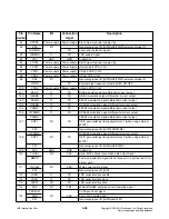
60
ASENV/LPPM
O
ASENV output/LPP mark output pin
61
LPPS
O
LPP space output pin
62
CLUMPGT
I
RFAGC input bias circuit clamp setting input pin (pulldown)
63 WBL
O
WBL binary
output
64 NC -
-
65
EQOUTA
O
Equalizer filter output pin 1.
66
EQOUTB
O
Equalizer filter output pin 2.
67
VCC22
PS
Power supply pin for RFEQ/LPP (5.0V)
68
FLTAMP
I
Filter final stage AMP reference voltage stabilization pin.
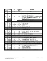
69
PAD0
I
A/D input pin 0
70
PAD1
I
A/D input pin 1
71
PAD2
I
A/D input pin 2
72
PAD3
I
A/D input pin 3
73 NC -
-
74 NC- -
-
75
CWBLHPF1
I
HPF capacitor connection pin for WBLAGC 1.
76
CWBLHPF2
I
HPF capacitor connection pin for WBLAGC 2.
77 NC -
-

