


9
Motherboard Information
Chapter 3
Network Application Platforms
Chapter 3:
Motherboard Information
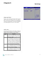
Block Diagram
The block diagram depicts the relationships among the
interfaces or modules on the motherboard. Please refer
to the following figure for your motherboard’s layout
design.
1x DDR3
667/800Mhz SO-DIMM
X4 DMI
Intel
82583V
Intel
82574L
Intel
82583V
Intel
82583V
Intel
82583V
Intel
82583V
6x PCI-E
x1
VGA
Up to 4GB
MAX
2 x SATA II
USB 2.0
Winbond
W83627DHG-P
RJ45 Console
Port
KB/Mouse
LPC
1 x 2.5" HDD
Bay supported
on the system
Console Pin
header
D525 Processor
CFII socket
2x USB 2.0
2x USB 2.0
Pin Header
Mini PCI-E socket
2 x 6 Pin Header
1 pair bypass on models A/C


