1-20 (No.RA020<Rev.002>)
2.4.5.2
VCO
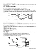
There are TX VCO and RX VCO.
The TX VCO (Q107) generates the carrier for the transmitter. The VCO oscillation frequency range is 136 to 174MHz. The transmit
frequency range is 136 to 174MHz.
The RX VCO (Q105) generates the 1st local signal for the receiver.
The VCO oscillation frequency range is 185.95 to 223.95MHz. The 1st local signal frequency range is 185.95 to 223.95MHz.
The VCO oscillation frequency is determined by voltage control terminals "CV" and "ASSIST".
The voltage control terminal "CV" is controlled by PLL IC (IC100). The voltage control terminal "ASSIST" is controlled by the control
voltage from D/A converter (IC715).
For the modulation input terminal, "VCO_MOD" of TX VCO, the output frequency changes according to the applied voltage. This is
used to modulate the VCO output.
2.4.5.3
PLL IC
PLL IC (IC100) compare the difference in phases of the VCO oscillation signal and the TCXO reference frequency. And it returns the
difference voltage to the VCO CV terminal and realizes the "Phase Locked Loop".
This allows the VCO oscillation frequency to accurately match (lock) the desired frequency.
When the frequency is controlled by the PLL, the frequency convergence time increases as the frequency difference increases when
the set frequency is changed. To supplement this, the MPU is used before control by the PLL IC to bring the VCO oscillation frequency
close to the desired frequency. As a result, the VCO CV voltage does not change and is always stable at approx. 2.5V.
The desired frequency is set for the PLL IC by the MPU (IC706) through the 3-line "SDO1", "P_SCK1", "/PCS_RF" serial bus for PLL.
MPU monitors through the “PLD”, whether the PLL IC is locked or not. If the VCO does not lock to desired frequency (unlock), the
“PLD” logic is low.
2.4.6 Control Circuit
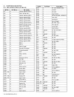
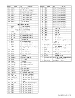
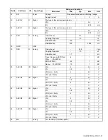
The control circuit consists of MPU/DSP (IC706) and its peripheral circuits. IC706 mainly performs the following;
(1) Switching between transmission and reception by PTT signal input.
(2) Reading system, zone, frequency, and program data from the memory circuit.
(3) Sending frequency program data to the PLL.
(4) Controlling the audio mute circuit by decode data input.
2.4.6.1
MPU
The MPU/DSP (IC706) is 32bit RISC processor and fixed floating-Point VLIW DSP Fixed/Floating-Point VLIW DSP, equipped with
peripheral function.
This MPU operates at 288MHz (MAX) clock and 3.3V/1.8V/1.2V DC. Controls the flash memory, Mobile DDR, the receive circuit, the
transmitter circuit, the control circuit, and the display circuit and transfers data to or from an external device.
2.4.6.2
Memory Circuit
Memory circuit consists of the MPU and the Mobile DDR (IC702), the flash memory (IC701). The flash memory has capacity of 512Mbit
that contains the transceiver control program for the MPU and stores the data.
It also stores the data for transceiver channels and operating parameter that are written by the FPU. This program can be easily written
from external devices. The Mobile DDR has capacity of 512Mbit. The MPU copies the program to the Mobile DDR from Flash memory.
And MPU is used as a work area Mobile DDR.
Flash memory
Note:
The flash memory stores the data that is written by the FPU (KPG-D1/D1N), tuning data (Deviation, Squelch, etc.) , and firmware
program (User mode, Test mode, Tuning mode, etc.). This data must be rewritten when replacing the flash memory.
Mobile DDR (static memory)
Note:
Mobile DDR is used as a work area of the MPU.
2.4.6.3
LCD
LCD interface connector (CN4) of the display unit.
The LCD is controlled using parallel interface from MPU (IC706) through the interface connectors (CN749 of the main unit and CN6
of display unit) and flexible cable.
2.4.6.4
Key Detection Circuit
Keys are detected using I/O Expander IC (IC10) of the display unit. If pressed key is detected by IC10, it is informed to MPU (IC706)
of the main unit through serial line.
Summary of Contents for NX-5700
Page 106: ...MEMO ...
Page 137: ...MEMO ...

