NX-720
23
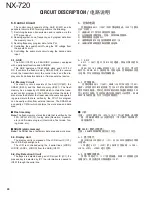
When the frequency is controlled by the PLL , the fre-
quency convergence time increases as the frequency dif-
ference increases when the set frequency is changed. To
supplement this, the ASIC (IC507) is used before control by
the PLL IC to bring the VCO oscillation frequency close to
the desired frequency. As a result, the VCO CV voltage does
not change and is always stable at approximately 2.5V.
The desired frequency is set for the PLL IC by the ASIC
(IC507) through the 3-line "SDO1", "P_SCK1", "/PCS_RF"
serial bus. Whether the PLL IC is locked or not is monitored
by the ASIC through the “PLD” signal line. If the VCO is not
the desired frequency (unlocked), the "PLD" logic is low.
The modulation signal of the Low-speed-Data is applied
to pin 23 of the PLL IC (IC2).
The modulation signal that is digital data of a sampling
frequency of
9
6 kHz is set for the PLL IC by the DSP (IC502)
through the “PLL_MOD” line.
5-4. Local Switch (D16, D17)
The connection destination of the signal output from the
buffer amplifi er (Q11) is changed with the diode switch (D17)
that is controlled by the transmission power supply, HSW,
and the diode switch (D16) that is controlled by the reception
power supply, 50R. If the HSW logic is high, it is connected
to a transmit-side drive (Q102). If the HSW logic is low, it is
connected to a receive-side mixer (Q202).
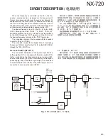
T/ R
SW
HSW
50
R
D16,17
BUFF
AMP
BUFF
AMP
Q11
Q10
VCO
Q6,7
D4,5,7,8,9
D10,11,12
D15
PLL
Loop
Filter
VCO MOD
ASSIST
CV
TCXO
X1 16.8MHz
SDO1
PCK_RF
/PCS RF
PLLMOD
IC2
IC3(2/2)
IC3(1/2)
50
CS
150C
to 1
st
MIXer
to TX stage
BPF
Doubler
Q5
CIRCUIT DESCRIPTION /
电路说明
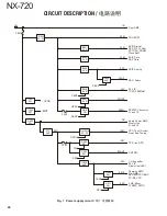
Fig. 6 PLL circuit /
图 6 PLL 电路
频率由 P L L 控制时,频率锁定时间将随着设定频率改变时
频率差的增大而增加。为对此进行补充,在由 PLL IC 控制之
前使用 ASIC (IC507) 以使 VCO 震荡频率接近所需的频率。因
此,VCO CV 的电压不变,始终稳定在约 2.5V。
PLL IC 的所需频率由 ASIC (IC507) 通过 3 线“SDO1”
、
“P_
SCK1”
、
“/PCS_RF”串行总线进行设置。PLL IC 是否锁定由
ASIC 通过“PLD”信号线路进行监测。如果 VCO 不是所需的频
率 ( 失锁 ),则“PLD”逻辑变低。
低速数据调制信号被加载到 PLL IC (IC2) 的第 23 脚。
调制信号是 DSP (IC502) 通过“PLL_MOD”线路为 PLL IC
设置的 96kHz 采样频率的数字数据。
5-4. 本振开关 (D16,D17)
缓冲放大器 (Q11) 输出信号的连接目标由发射电源 H S W
控制的二极管开关 (D17) 和接收电源 50R 控制的二极管开关
(D16) 进行切换。如果 HSW 逻辑为高,则被连接到发送侧驱动
(Q102)。如果 HSW 逻辑为低,
则被连接到接收侧混频器 (Q202)。
Summary of Contents for NEXEDGE NX-720
Page 122: ...NX 720 ...


