

TH-V70
1-53
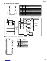
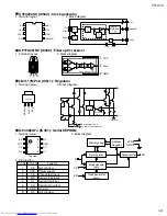
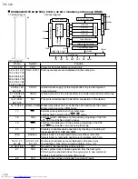
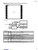
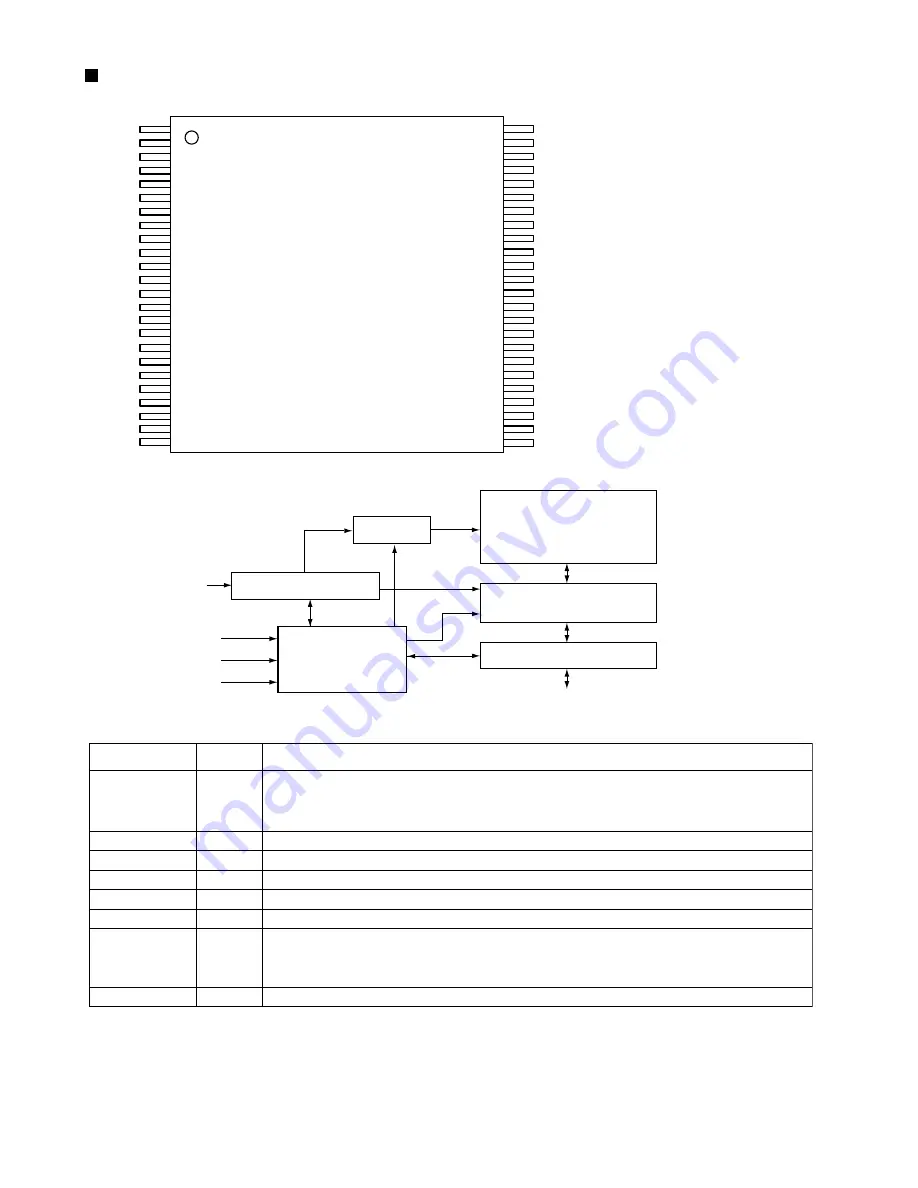
1. Terminal layout
SST39VF160-7CEK (IC509) : 16 Mbit multi-purpose flash memory
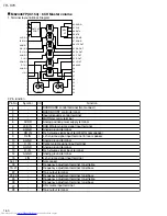
2. Block diagram
Y-Decoder
I/O Buffers and Data Latches
Address buffer & Latches
D15 - D0
Memory Address
/OE
/CE
/WE
Super flash memory
Control Logic
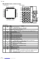
Top view
A15
A14
A13
A12
A11
A10
A9
A8
A19
NC
/WE
*/RST
NC
NC
*R/B
A18
A17
A7
A6
A5
A4
A3
A2
A1
1
2
3
4
5
6
7
8
9
10
11
12
13
14
15
16
17
18
19
20
21
22
23
24
48
47
46
45
44
43
42
41
40
39
38
37
36
35
34
33
32
31
30
29
28
27
26
25
A16
*/BYTE
VSS
D15
D7
D14
D6
D13
D5
D12
D4
VCC
D11
D3
D10
D2
D9
D1
D8
D0
/OE
VSS
/CE
A0
X-Decoder
1 - 9,
16 - 25,48
10,12 - 15,47
11
26
27,46
28
29 - 36, 38 - 45
37
A19 - A0
NC
/WE
/CE
VSS
/OE
D15 - D0
VCC
Address inputs : To provide memory addresses.
During Sector-Erase A19 - A11 address lines will select the sector.
During Block-Erase, A19 - A15 address line will select the block.
No connection : Unconnected pins
Write Enable : To control the Write operations
Chip Enable : To activate the device when CE# is low
Ground
Output Enable : To gate the data output buffers
Data input/output : To output data during Read cycles and receive input data
during write cycles. Data is internally latched during a write cycle. The outputs are
in tri-state when OE# or CE# is high.
Power supply : To provide power supply voltage (2.7 - 3.6V)
Pin No.
Symbol
Function
3. Pin function
Summary of Contents for TH-V70
Page 55: ...TH V70 1 55 M E M O ...


