

TH-V70
1-28
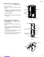
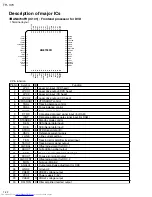
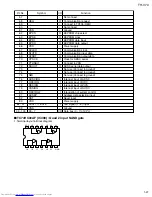
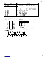
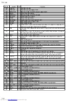
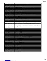
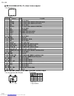
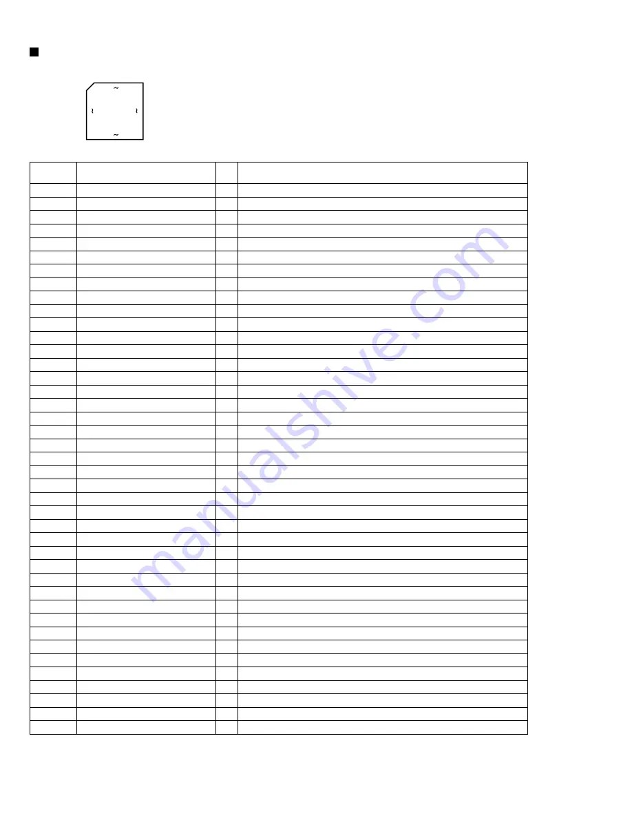
1.Terminal layout
MN103S26EGA (IC301) : Optical disc controller
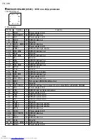
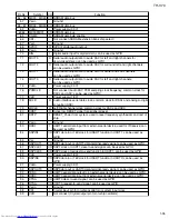
Pin No.
Symbol
2. Pin function
I/O
NINT0
NINT1
VDD3
VSS
NINT2
WAITODC
NMRST
DASPST
CPUADR17 - 9
VDD18
VSS
DRAMVDD18
DRAMVSS
CPUADR8 - 0
VDD3
VSS
DRAMVDD3
NCS
NWR
NRD
CPUDT7 - 0
CLKOUT1
MMOD
NRST
MSTPOL
SCLOCK
SDATA
OFTR
BDO
PWM1 - 4
VDD3
DRAMVDD18
DRAMVSS
VSS
PWM5 - 8
TBAL
FBAL
TRSDRV
SPDRV
FG
TILTP
O
O
-
-
O
O
-
-
I
-
-
-
-
I
-
-
-
I
I
I
I/O
-
I
I
I
-
-
I
I
-
-
-
-
-
-
O
O
O
O
I
-
System control interruption 0
System control interruption 1
Power supply (3.3V)
Ground
System control interruption 2
System control wait control
System control reset (Not connect)
DASP signal initializing
System control address
Power supply (1.8V)
Ground
Connect to VDD18
Connect to VSS
System control address
Power supply (3.3V)
Ground
Connect to VDD3
System control chip select
System control write
System control read
System control data
Not connect
Connect to VSS
System reset
Master terminal polarity switch input
Not connect
Not connect
Off track signal input
RF dropout/BCA data of making to binary
Not connect
Power supply (3.3V)
Connect to VDD18
Connect to VSS
Ground
Not connect
Tracking balance adjustment output
Focus balance adjustment output
Traverse drive output
Spindle drive output
Motor FG input
Not connect
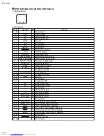
1
44
132
89
176 133
45 88
1
2
3
4
5
6
7
8
9 - 17
18
19
20
21
22 - 30
31
32
33
34
35
36
37 - 44
45
46
47
48
49
50
51
52
53 - 56
57
58
59
60
61 - 64
65
66
67
68
69
70
Function
Summary of Contents for TH-V70
Page 55: ...TH V70 1 55 M E M O ...


