background image

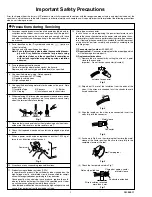
Important Safety Precautions

Prior to shipment from the factory, JVC products are strictly inspected to conform with the recognized product safety and electrical codes of the
countries in which they are to be sold. However, in order to maintain such compliance, it is equally important to implement the following precautions
when a set is being serviced.

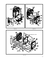
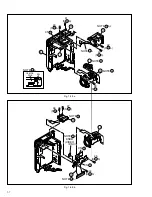
Fig.1

1. Locations requiring special caution are denoted by labels and in-

scriptions on the cabinet, chassis and certain parts of the product.
When performing service, be sure to read and comply with these
and other cautionary notices appearing in the operation and serv-
ice manuals.

2. Parts identified by the 

!

 symbol and shaded (        ) parts are

critical for safety.
Replace only with specified part numbers.

Note: Parts in this category also include those specified to com-

ply with X-ray emission standards for products using
cathode ray tubes and those specified for compliance
with various regulations regarding spurious radiation
emission.

3. Fuse replacement caution notice.

Caution for continued protection against fire hazard.
Replace only with same type and rated fuse(s) as specified.

4. Use specified internal wiring. Note especially:

1) Wires covered with PVC tubing
2) Double insulated wires
3) High voltage leads

5. Use specified insulating materials for hazardous live parts. Note

especially:
1) Insulation Tape

3) Spacers

5) Barrier

2) PVC tubing

4) Insulation sheets for transistors

6. When replacing AC primary side components (transformers, power

cords, noise blocking capacitors, etc.) wrap ends of wires securely
about the terminals before soldering.

Power cord

Fig.2

10. Also check areas surrounding repaired locations.

11. Products using cathode ray tubes (CRTs)

In regard to such products, the cathode ray tubes themselves, the
high voltage circuits, and related circuits are specified for compli-
ance with recognized codes pertaining to X-ray emission.
Consequently, when servicing these products, replace the cath-
ode ray tubes and other parts with only the specified parts. Under
no circumstances attempt to modify these circuits.
Unauthorized modification can increase the high voltage value and
cause X-ray emission from the cathode ray tube.

12. Crimp type wire connector

In such cases as when replacing the power transformer in sets
where the connections between the power cord and power trans-
former primary lead wires are performed using crimp type connec-
tors, if replacing the connectors is unavoidable, in order to prevent
safety hazards, perform carefully and precisely according to the
following steps.

1) Connector part number : 

E03830-001

2) Required tool : 

Connector crimping tool of the proper type which

will not damage insulated parts.

3) Replacement procedure

(1) Remove the old connector by cutting the wires at a point

close to the connector.
Important : Do not reuse a connector (discard it).

Fig.7

cut close to connector

Fig.3

(2) Strip about 15 mm of the insulation from the ends of the

wires. If the wires are stranded, twist the strands to avoid
frayed conductors.

15 mm

Fig.4

(3) Align the lengths of the wires to be connected. Insert the

wires fully into the connector.

Connector

Metal sleeve

Fig.5

(4) As shown in Fig.6, use the crimping tool to crimp the metal

sleeve at the center position. Be sure to crimp fully to the
complete closure of the tool.

I


Precautions during Servicing

7. Observe that wires do not contact heat producing parts (heatsinks,

oxide metal film resistors, fusible resistors, etc.)

8. Check that replaced wires do not contact sharp edged or pointed

parts.

9. When a power cord has been replaced, check that 10-15 kg of

force in any direction will not loosen it.

1.2

5

2.0

5.5

Crimping tool

Fig.6

(5) Check the four points noted in Fig.7.

Not easily pulled free

Crimped at approx. center

of metal sleeve

Conductors extended

Wire insulation recessed

more than 4 mm

S40888-01

Summary of Contents for GR-DVP7U

Page 1: ...A Weight Approx 255 g 0 57 lbs Specifications shown are for SP mode unless otherwise indicated E O E Design and specifications subject to change without notice Camcorder For General Power supply DC 6 3 V Using AC Power Adapter Charger DC 7 2 V Using battery pack Power consumption LCD monitor off viewfinder on Approx 4 2 W LCD monitor on viewfinder off Approx 5 0 W Dimensions W x H x D 43 mm x 115 ...

Page 2: ... Adjustment of the Slide Lever 2 2 16 2 7 SERVICE NOTE 2 17 2 8 COMPATIBILITY ADJUSTMENT 2 19 2 8 1 Jig connector cable connection 2 19 2 8 2 Tape pattern check 2 19 TABLE OF CONTENTS Section Title Page Section Title Page 3 ELECTRICAL ADJUSTMENT 3 1 PRECAUTION 3 1 3 2 SETUP 3 2 4 CHARTS AND DIAGRAMS NOTES OF SCHEMATIC DIAGRAM 4 1 CIRCUIT BOARD NOTES 4 2 4 1 BOARD INTERCONNECTIONS 4 3 4 2 SYSCON CP...

Page 3: ...e specified for compli ance with recognized codes pertaining to X ray emission Consequently when servicing these products replace the cath ode ray tubes and other parts with only the specified parts Under no circumstances attempt to modify these circuits Unauthorized modification can increase the high voltage value and cause X ray emission from the cathode ray tube 12 Crimp type wire connector In ...

Page 4: ... between terminals and surrounding metallic parts See table 1 below 4 Leakage current test Confirm specified or lower leakage current between earth ground power cord plug prongs and externally exposed accessible parts RF terminals antenna terminals video and audio input and output terminals microphone jacks earphone jacks etc Measuring Method Power ON Insert load Z between earth ground power cord ...

Page 5: ...icates the name of disassembly assembly parts 3 Indicates the number in the disassembly diagram 4 Indicates parts and points such as screws washers springs which must be removed during disassembly assembly Symbol Name Point S Screw L Lock Pawl Hook SD Soldering CN Connector Example 2 S1 Remove the two screws S1 for removing the part 1 CN 1a Disconnect the connector 1a SD 1 Unsolder at the point SD...

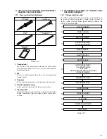
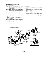
Page 6: ...nsport system optical lens surface 1 3 DISASSEMBLY ASSEMBLY OF CABINET PARTS AND BOARD ASSEMBLY 1 3 1 Disassembly flow chart This flowchart indicates the disassembly step for the cabi net parts and board assembly in order to gain access to item s to be serviced When reassembling perform the step s in reverse order Table 1 2 1 Table 1 3 1 Torque driver YTU94088 1 Bit YTU94088 003 2 3 Chip IC replac...

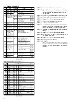
Page 7: ...over MULTI USB NOTE 4d Slide down the shutter and remove the screw 15 NOTE 5 Refer to Fig 1 4 1 for the disassembly method NOTE 6 Be careful not to damage or lose the parts NOTE 7 Take care of the removed screws NOTE 8 For the disassembly assembly of the E VF unit Shoe assembly OP MDA board assembly and OP block as sembly see section 1 8 SERVICE KNOW HOW NOTE Leave the microphone connected to the ...

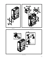
Page 8: ...1 4 Fig 1 3 2 Fig 1 3 3a Fig 1 3 1 1 S 1 1 S a 4 3 S b 5 3 S b 6 3 S 3 2 S 2 2 L 2 2 3 NOTE a 4 NOTE b 4 BATT RELEASE SWITCH COVER SD 4 LOCK LEVER ...

Page 9: ... 4 S c 13 4 S d 12 4 CN a 4 CN COVER M USB b 4 NOTE c 4 S e 14 NOTE d 4 4 S b 8 4 S c 10 4 S c 9 4 S e 16 4 S f 15 4 0 118 N m 1 2 kgf cm 4 5 S a 17 GUIDE MONI 5 NOTE 5 S b 20 5 S a 18 5 S b 19 5 0 098 N m 1 0 kgf cm 6 S 21 6 NOTE 6 Fig 1 3 5 ...

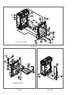
Page 10: ...2 8 S 33 SHIELD ASSY BRACKET PRE REC BRACKET MECHA ASSY SHEET SHUTTER 9 S b 38 10 CN a 9 CN d 9 CN b 9 CN c 9 L b 9 S b 36 10 S b 37 10 S a 35 10 S 34 9 L a 9 9 10 CN e 9 CN f 9 Fig 1 3 7 NOTE 7 S a 23 7 S b 7 24 S b 7 25 CASS COVER S a 22 7 S a 23 7 S b 24 7 S b 25 7 S c 26 7 S c 27 7 CN 7 S c 28 7 S d 29 7 7 ...

Page 11: ... 8 12 15 13 NOTE 11 NOTE 12 NOTE OP MDA PWB a 13 NOTE a 13 NOTE b c 13 CN 13 S b 43 13 S a 42 13 14 SW S a 40 14 S a 41 14 S 39 12 14 12 15 S b 44 14 CN 12 NOTE b 14 NOTE a 14 NOTE 15 CN 15 S b 45 14 S 46 15 S 47 15 KNOB VIDEO DSC ...

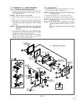
Page 12: ...the connector CN5b and remove the LCD module Be careful with the hooks L5g L5h on the two sides 1 4 2 Hinge assembly 1 Remove the two screws 4 5 to take out the FPC assem bly while removing the hinge cover L Note5c Be careful not to lose any part during the above mentioned process 2 Remove the hinge cover U from hinge assembly 3 Remove the FPC assembly from the hinge assembly Note5d Be careful not...

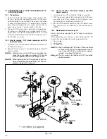
Page 13: ... don t re place it individually but replace the CCD base as sembly in whole with a new one 1 5 3 How to install OP block assembly and CCD board assembly 1 Install the optical LPF with the OP block assembly 2 With the spacer rubber left attached to the CCD base assembly install the assembly in the OP block assem bly and clamp it using the two screws 1 2 3 Set the CCD board assembly in the CCD base ...

Page 14: ...y Note c A lens assembly and a lever are mounted on the eye piece sub assembly When removing this as sembly be careful not to damage them 5 Draw out the guide VF Frame VF 6 Remove the screw 6 first and then LCD module holder LCD 7 Get the two hooks L a L b disengaged and then re move the holder LCD Note d Carefully proceed with the above mentioned work not to damage any part 8 Disconnect the conne...

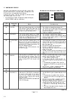
Page 15: ...s locked during mode shift 2 The mechanism is locked at the mechanism loading end because the encoder position is skipped during mechanism mode shift E03 TU SUP REEL FG In the case no REEL FG is produced for 4 sec onds or more in the capstan rotation mode af ter loading was complete the mechanism mode is shifted to STOP with the pinch roller set off This error is defined as E03 However no REEL EMG...

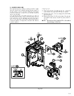
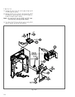
Page 16: ...conven iently This section gives further details regarding the disas sembly procedures although they have been described in previous sections 1 See Fig 1 8 1 1 While moving the microphone out of way remove the screw 39 and take out the OP block assembly 2 Remove two screws 40 41 and open the OP MDA board assembly 3 Remove two screws 42 43 to disconnect the connec tor CN203 then take out the FPC to...

Page 17: ...ssembly together with the OP block as sembly and the shoe assembly Note Be careful not to lose the VIDEO and DSC knobs which may slip out during the disassembly 3 Disconnect the FPCs from the connectors on the OP block assembly and the shoe assembly Fig 1 8 2 14 12 15 S b 44 14 CN 12 NOTE 12 NOTE b 14 NOTE 15 CN 15 S b 45 14 S 46 15 S 47 15 KNOB VIDEO DSC ...

Page 18: ...awing Screw tightening torque NOTE 1 Don t reuse the screw because screw lock bond was applied to them 2 Pay careful attention to tightening torque for each screw I 0 078N m 0 8kgf cm II 0 118N m 1 2kgf cm III 0 098N m 1 0kgf cm IV 0 069N m 0 7kgf cm V 0 058N m 0 6kgf cm 1 2 3 4 5 6 7 8 9 10 11 12 13 14 15 16 17 18 19 20 21 1 2 3 7 8 9 0 5 4 5 6 I I I I III II 22 23 24 25 26 27 28 29 30 31 32 33 3...

Page 19: ...rs in this column correspond to those appearing in drawings of this section 2 This column shows part names corresponding to circled numbers in the left column 3 The symbol T or B appearing in this column shows the side which the objective part is mounted on T the upper side B the lower side 4 Symbols appearing in this column indicate drawing numbers Step Part Name Fig Point Note Remarks 5 This col...

Page 20: ...puter with each other when a personal computer is used for adjustment 11 Alignment tape To be used for check and adjustment of interchange ability of the mechanism 12 Service support system To be used for adjustment with a personal computer 13 Cassette torque meter This is used to cheek the back tension and play torque during mechanism adjustment Note When using the cassette torque meter install t...

Page 21: ...assembled assem bled in the C IN mode ASSEMBLY mode Refer to Fig 2 3 1 2 However when the mechanism is removed from the main body it is set in the STOP mode Therefore after the mechanism is removed from the main body supply 3 V DC to the electrode on the top of the loading motor to enter the mechanism mode into the C IN mode compulsory Mechanism assembly Cassette housing assembly Back side of the ...

Page 22: ...110 06 206 06 210 05 80 34 0 243 29 291 16 333 82 292 310 74 L END LOCK OFF TU ARM ON OFF SLIDE DECK LOAD UL BRAKE S ON OFF BRAKE T ON OFF RELEASE LEVER ROTARY ENCODER MAIN CAM SUB CAM ON a OFF CTL PLATE C R L TENSION ARM UL L END OFF PAD ARM UL L END LOAD SUP L ARM UL L END LOAD TU L ARM UL PRESS LOAD P ROLLER UL b c CAS IN SHORT STOP PLAY REV FWD TU P B START TU P B END END SLIDE SLIDE START 2 3...

Page 23: ... F ASSY T W NOTE 18 TENSION CTL PLATE ASSY T NOTE ADJUSTMENT 19 BRAKE CTL LEVER ASSY T NOTE ADJUSTMENT 20 MOTOR BRACKET ASSY T Fig 2 4 9 3 S L a 2 L b NOTE ADJUSTMENT 21 GUIDE RAIL ASSY T 2 W S 2 L a L b NOTE ADJUSTMENT 22 SLIDE LEVER 2 ASSY T NOTE ADJUSTMENT 夝 23 LOADING PLATE ASSY T W NOTE ADJUSTMENT 24 MODE GEAR T NOTE 25 EJECT LEVER T Wfi NOTEfi ADJUSTMENT 26 BASE R ASSY T Fig 2 4 10 Sfla Sflb 2 L...

Page 24: ...2 6 Fig 2 4 1 Fig 2 4 2 24 27 2 3 36 35 21 26 17 34 9 10 33 26 6 5 25 11 32 37 14 31 28 16 15 30 29 13 4 12 7 8 22 18 23 20 19 34 26 32 31 16 6 30 30 25 36 3 22 27 20 37 18 29 11 19 TOP VIEW BOTTOM VIEW ...

Page 25: ...ER 1 NOTE d 1 NOTE1c When mounting the CASSETTE HOUSING ASSY should be at tached in the Eject status Pay heed to the positions of the LOCK LEVER and EJECT LEVER during mounting NOTE1a Be careful not to damage any of the parts during work NOTE1b Special care is required in mounting NOTE1d When mounting be sure to locate the FPC in the gap NOTE 2 5 6 7 NOTE 3 b NOTE2 When mounting be sure to insert ...

Page 26: ...ful not to lose the spring NOTE 8 SPRING A B NOTE 9 NOTE 10 NOTE6 Perform the following steps for mounting 1 Align the 2 holes with the pins 2 Attach the PINCH ROLLER ARM ASSY by aligning the positions 3 Attach the SUB DECK ASSY by aligning the positions 4 Check that the parts below them are lo cated in the correct positions 5 Tighten the 2 screws 6 Tighten the screw 7 Attach the 2 SLIT WASHER par...

Page 27: ... need to replace any of its parts remove the SLIDE DECK ASSY as it is NOTE b When mounting pay attention to the positions of the SLIDE LEVER 2 studs and the BRAKE CONTROL LE VER ASSY When mounting position the CONTROL PLATE on the left side Pay attention to the position of the SLIDE GUIDE PLATE during mounting NOTE 12 13 14 12 13 14 SPRING CONTROL PLATE NOTE The spring may have already been diseng...

Page 28: ...25 L b 20 L a 20 L a 21 L b 21 NOTE 24 NOTE 22 NOTE 21 NOTE 23 NOTE 20 NOTE 25 NOTE 18 NOTE 19 NOTE 20 NOTE 21 NOTE 22 NOTE 15 NOTE 17 NOTE Take care against grease attachment during work NOTES When mounting pay attention to the correct positioning NOTE 16 TOP BOTTOM NOTES When mounting pay atten tion to the correct position ing NOTE When mounting pay attention to the position ing of the sliding p...

Page 29: ...TE 32 NOTE 34 NOTEfl When mounting fold the sliding part to the inner side NOTE When mounting pay attention to the correct positioning NOTE When mounting pay attention to the correct positioning and the FPC layout NOTE When mounting pay attention to the correct positioning and the FPC lay out NOTES When mounting pay attention to the correct positioning and the FPC layout NOTE When mounting pay atte...

Page 30: ...TE 35 a NOTE 36 11 DRUM BASE ASSY CAPSTAN MOTOR MAIN DECK ASSY Z27 Ver 5_N NG OK NG NOTE b 35 NOTES a When detaching remove them together and then separate from NOTE b When mounting attach the DRUM BASE ASSY so that the screw hole is located at the center of the ellipse ...

Page 31: ...12 14 11 5 4 1 S 1 S b 2 S 1 W 4 W 6 W 12 P 12 P 8 P 14 P 13 15 S 13 W 14 W 21 W 23 W 21 W 25 W 17 W 6 W 5 1 S 10 11 S 2 4 S 1 3 S 21 19 S 20 18 S 20 17 S 20 16 S 27 23 S 35 28 S 35 29 S 36 31 S 35 30 S 32 27 S 27 22 7 3 S b 14 11 S a 12 11 S a 13 11 S b 6 3 S a 20 26 S b 25 28 S b 26 28 S a 24 28 S a 5 3 S b 10 6 S a 9 6 S a 8 6 S b 21 26 W 15 ...

Page 32: ...osition SUB CAM ASSY 33 CONTROL ARM ASSY Mount the SUB CAM ASSY hole to align with the CONTROL ARM ASSY and Main Deck Assembly holes and then tighten them all together with a screw The screw tightening torque should be 0 039 N m 0 4 kgf cm Note When mounting it make sure that the 29 MAIN CAM ASSY is in the correct mounting position REEL GEAR 1 Align the REEL GEAR 1 with the Main Deck Assembly hole...

Page 33: ...into the unit tighten the screws A B while applying pressure to the stud shaft on the Slide Guide plate The pressure applied should be enough to enable utili zation of the rebounding force of the springs The tightening torque should be 0 069 N m 0 7 kgf cm 4 Check the operation Repeat unloading and loading several times and make sure that these operations can be performed smoothly without producin...

Page 34: ...se Fig 2 6 2 as the reference unless otherwise specified 1 Set the PLAY mode Se Fig 2 3 8 2 Loosen the screw A 3 With the take up side at the bottom align the extreme end of the Tension Arm Assembly with the crossed grooves on the screw B that retains the Loading Motor Assembly and then tighten the screw A The tightening torque should be 0 069 N m 0 7 kgf cm 4 Check the operation Repeat unloading ...

Page 35: ... I 4 I 4 CASSETTE HOUSING ASSY UPPER BASE ASSY DRUM ASSY 2 I 4 I 4 2 I 4 I 5 2 I 4 I 6 REEL DISK ASSY SUP REEL DISK ASSY TU TENSION ARM ASSY SLIDE DECK ASSY SLANT POLE ARM ASSY SWING ARM ASSY TU ARM ASSY PAD ARM ASSY SUP BRAKE ASSY TU BRAKE ASSY REEL COVER ASSY 2 I 4 I 7 a 2 I 4 I 7 b Fig Fig Fig Fig Fig Fig Fig 2 3 6 7 8 9 10 13 12 14 11 5 4 1 ...

Page 36: ...ET ASSY BASE R ASSY ROTARY ENCODER GEAR COVER ASSY DRUM BASE ASSY SLIDE ARM ASSY CONNECT GEAR 2 SUB CAM ASSY CONTROL ARM ASSY REEL GEAR 1 CAPSTAN MOTOR MAIN DECK ASSY MAIN CAM ASSY GUIDE RAIL ASSY SLIDE LEVER 2 ASSY LOADING PLATE ASSY MODE GEAR EJECT LEVER BRAKE CTL LEVER ASSY Fig Fig Fig Fig Fig 18 24 30 32 34 36 35 33 31 20 21 37 25 26 27 29 28 23 22 17 16 19 15 ...

Page 37: ...n played back again play back the self recording to confirm that the waveform is flat Fig 2 8 3 Fig 2 8 4 CN114 29 ENV_OUT CN114 11 HID1 Flatten the waveform Misalignment of guide roller height on the take up side Misalignment of guide roller height on the supply side Note When an adjustment is performed with the lower case cover attached first slide the Cover M ADJ open and then per form the comp...

Page 38: ... them in dis connecting and connecting 3 Shortcircuit between operation un it and DECK chassis 2 Required test equipment 1 Color TV monitor 2 AC power adapter charger 3 Oscilloscope dual trace type observable 100 MHz or higher frequency Note It is recommended to use one observable 300 MHz or higher frequency 4 Digital voltmeter 5 Frequency counter with threshold level adjuster 6 Personal computer ...

Page 39: ...Fig 3 2 1 Connection for Service support system 9 Service support system To be used for adjustment with a personal computer 10 INF adjustment lens To be used for adjustment of the camera system 11 INF adjustment lens holder To be used together with the camera stand for operat ing the VideoMovie in the stripped down condition such as the status without the exterior parts or for using com modities t...

Page 40: ...ER CHARER AA V100U 21 LY32226 002A DC CORD ASSY 22 QQR0917 002 CORE FILTER 23 QAM0403 001 MULTI CABLE S AV EDITING CABLE 25 QAM0387 001 USB CABLE 27 QAM0402 001 RM CABLE EDITING EXTENSION CABLE 35 LY32203 003A BATTERY PACK BN V107U S 36 LY20750 001A REMOTE CONTROL UNIT RM V717U 37 LY32210 026A CD ROM ASSY 38 LY20762 001B GRIP BELT 39 LY20892 001A STRAP 40 BATTERY AAA R03 X2 41 QPA01703005 POLY BAG...

Page 41: ... 229 237 236A k d bb n p s m r q t w u v p n x y z gg aa s t q r ff aa 236 238 238 238 229 152 152A 152B 152C 153 174 174 173 151 192 194 193 185 185A 185A 185A 186 186 186 187 187 190 191 189 188 189 188A MECHANISM M3 MAIN 01 164 166 121 122 165 159 161 160 154 MONITOR M5 175 e b z f BOTTOM 03 OP MDA 02 243 243 ee cc bb dd ff 175 159 160 150 170 hh k c u v c 168 150A 150B 168 171 171 169 f e x g ...

Page 42: ...LY41836 001A SPACER 185 LY43435 001B MECHA BRACKET ASSY 185A LY42796 001A BUSH X3 185B LY43769 001A MECHA ARM SHEET 186 LY30019 028A SPECIAL SCREW X3 187 LY30018 055A SPECIAL SCREW X2 188 LY43190 001A SHIELD ASSY 188A LY43189 001A SPACER 189 LY30018 005A SPECIAL SCREW X2 190 LY43083 001A BRACKET PRE REC 191 LY30018 0G3A SCREW 192 LY43612 001A SHUTTER B SHEET 193 LY32001 002A LABEL HOUSING 194 LY40...

Page 43: ...453 431 436 437 437 425 424 437 436B 436A 436B 428 429 454 434 435 461 463 465 BB AA AA AA CC AA CC CC CC CC AA AA 400 430 476 AA Classification Part No Symbol in drawing Grease KYODO SH JB AA Oil YTU94027 BB Grease RX 410R CC HANARL NOTE The section marked in AA and BB CC indicate lubrication and greasing areas BEWARE OF BOGUS PARTS Parts that do not meet specifications may cause trouble in regar...

Page 44: ...525 001B CENTER GEAR 432 LY31516 001E PINCH ROLLER ARM FINAL ASSY 433 YQ44246 SLIT WASHER 434 LY41956 001C TENSION CONTROL PLATE ASSY 435 LY41962 001B BRAKE CONTROL LEVER ASSY 436 LY20525 002C MOTOR BRACKET ASSY 436A QAR0138 001 LOADING MOTOR 436B LY41940 001A TAPPING SCREW X2 437 YQ43893 MINI SCREW X3 438 LY20528 001R GUIDE RAIL ASSY 439 YQ43893 MINI SCREW 440 YQ44246 SLIT WASHER X2 441 LY31498 0...

Page 45: ...EW 321 LY30018 0D4A SPECIAL SCREW 322 QAL0411 001 FPC 323 LY43775 001A SPACER VF LCD 324 LY43824 001A SHEET VF ELECTRONIC VIEWFINDER ASSEMBLY M4 300 LYH20422 001C VF ASSY 301 LY32640 001A SLIDE GUIDE INNER ASSY 302 LY43451 001A LENS ASSY 303 LY32643 001B VF CASE ASSY 304 LY43454 001A BACKLIGHT CASE 305 LY43328 001A SHEET PRISM 306 LY43327 001A SHEET DIFFUSE 307 QLD0117 002 LCD MODULE 308 LY32646 0...

Page 46: ...PART NAME DESCRIPTION REF No PART No PART NAME DESCRIPTION 506 LY32267 002A HINGE COVER U 507 LY32268 002A HINGE C0VER L 508 LY42355 001A MAGNET 509 LY30018 0D9A SPECIAL SCREW X2 510 LY30018 043B SPECIAL SCREW 511 LY30018 0B7A SPECIAL SCREW X2 512 LY43523 001A MARK 513 LY30029 0N7A SPACER A 514 QLD0235 001 LCD MODULE 515 QLL0120 001 BACK LIGHT 516 LY32766 001A FPC ASSY MONI 518 LY30029 0X8A SPACER...

Page 47: ... TRANSISTOR or PDTA114EE DIGI TRANSISTOR or RN2102 DIGI TRANSISTOR or UN9111J DIGI TRANSISTOR Q1007 DTC144EE DIGI TRANSISTOR or PDTC144EE DIGI TRANSISTOR or RN1104 DIGI TRANSISTOR or UN9213J DIGI TRANSISTOR Q1401 DTA114EE DIGI TRANSISTOR or PDTA114EE DIGI TRANSISTOR or RN2102 DIGI TRANSISTOR or UN9111J DIGI TRANSISTOR Q1402 UMC3N DIGI TRANSISTOR Q1403 UMC3N DIGI TRANSISTOR Q1601 UMC3N DIGI TRANSIS...

Page 48: ...1 NRSA6AJ 473W MG RESISTOR 47kØ 1 16W R1066 NRSA6AJ 473W MG RESISTOR 47kØ 1 16W R1072 NRSA6AJ 104W MG RESISTOR 100kØ 1 16W R1076 NRSA6AJ 0R0W MG RESISTOR 0Ø 1 16W R1077 NRSA6AJ 0R0W MG RESISTOR 0Ø 1 16W R1084 NRSA6AJ 0R0W MG RESISTOR 0Ø 1 16W R1086 NRSA6AJ 103W MG RESISTOR 10kØ 1 16W R1087 NRSA6AJ 102W MG RESISTOR 1kØ 1 16W R1101 NRSA6AJ 333W MG RESISTOR 33kØ 1 16W R1102 NRSA6AJ 472W MG RESISTOR 4...

Page 49: ...0Ø 1 16W R2702 NRSA6AJ 821W MG RESISTOR 820Ø 1 16W R2703 NRSA6AJ 564W MG RESISTOR 560kØ 1 16W R2704 NRSA6AJ 564W MG RESISTOR 560kØ 1 16W R2705 NRSA6AJ 332W MG RESISTOR 3 3kØ 1 16W R2706 NRSA6AJ 221W MG RESISTOR 220Ø 1 16W R2707 NRSA6AJ 221W MG RESISTOR 220Ø 1 16W R2708 NRSA6AJ 103W MG RESISTOR 10kØ 1 16W R2709 NRSA6AJ 103W MG RESISTOR 10kØ 1 16W R2710 NRSA6AJ 332W MG RESISTOR 3 3kØ 1 16W R2711 NRS...

Page 50: ...ESISTOR 100Ø 1 16W R4311 NRSA6AJ 101W MG RESISTOR 100Ø 1 16W R4312 NRSA6AJ 101W MG RESISTOR 100Ø 1 16W R4313 NRSA6AJ 101W MG RESISTOR 100Ø 1 16W R4317 NRSA6AJ 0R0W MG RESISTOR 0Ø 1 16W R4318 NRSA6AJ 0R0W MG RESISTOR 0Ø 1 16W R4320 NRSA6AJ 0R0W MG RESISTOR 0Ø 1 16W R4321 NRSA6AJ 0R0W MG RESISTOR 0Ø 1 16W R4322 NRSA6AJ 0R0W MG RESISTOR 0Ø 1 16W R4323 NRSA6AJ 0R0W MG RESISTOR 0Ø 1 16W R4324 NRSA6AJ 0...

Page 51: ...J 102W MG RESISTOR 1kØ 1 16W R8016 NRSA6AJ 103W MG RESISTOR 10kØ 1 16W R8017 NRSA6AJ 0R0W MG RESISTOR 0Ø 1 16W R8022 NRSA6AJ 105W MG RESISTOR 1MØ 1 16W R8037 NRSA6AJ 103W MG RESISTOR 10kØ 1 16W R8038 NRSA6AJ 220W MG RESISTOR 22Ø 1 16W R8043 NRSA6AJ 220W MG RESISTOR 22Ø 1 16W R8046 NRSA6AJ 0R0W MG RESISTOR 0Ø 1 16W R8049 NRSA6AJ 103W MG RESISTOR 10kØ 1 16W R8051 NRSA6AJ 103W MG RESISTOR 10kØ 1 16W ...

Page 52: ...2201 NCBA1AK 104W CAPACITOR 0 1µF 10V C2202 NCB30JK 105X CAPACITOR 1µF 6 3V C2203 NCB30JK 105X CAPACITOR 1µF 6 3V C2204 NCB30JK 105X CAPACITOR 1µF 6 3V C2205 NCB30JK 105X CAPACITOR 1µF 6 3V C2206 NBE20GM 476X T CAPACITOR 47µF 4 0V C2207 NBE20GM 476X T CAPACITOR 47µF 4 0V C2208 NCBA1AK 104W CAPACITOR 0 1µF 10V C2209 NCB30JK 105X CAPACITOR 1µF 6 3V C2210 NCB30JK 105X CAPACITOR 1µF 6 3V C2211 NCBA1AK...

Page 53: ...GM 226X T CAPACITOR 22µF 4 0V C3712 NBE20GM 107X T CAPACITOR 100µF 4 0V C3713 NBE20GM 107X T CAPACITOR 100µF 4 0V C3715 NCBA1CK 103W CAPACITOR 0 01µF 16V C3731 NCBA1CK 103W CAPACITOR 0 01µF 16V C3732 NCBA1HK 102W CAPACITOR 0 001µF 50V C3733 NDCA1HJ 3R0W CAPACITOR 3pF 50V C3734 NDCA1HJ 5R0W CAPACITOR 5pF 50V C3735 NDCA1HJ 330W CAPACITOR 33pF 50V C3736 NCBA1HK 102W CAPACITOR 0 001µF 50V C3738 NCBA1C...

Page 54: ...V C6123 NCB31CK 683X CAPACITOR 0 068µF 16V C6124 NCB21CK 105X CAPACITOR 1µF 16V C6125 NCB10JK 106X CAPACITOR 10µF 6 3V C6126 NCB21CK 105X CAPACITOR 1µF 16V C6127 NCB10JK 106X CAPACITOR 10µF 6 3V C6128 NCB21CK 105X CAPACITOR 1µF 16V C6129 NCB30JK 105X CAPACITOR 1µF 6 3V C6130 NCB21CK 105X CAPACITOR 1µF 16V C6131 NCB30JK 105X CAPACITOR 1µF 6 3V C6132 NCB21CK 105X CAPACITOR 1µF 16V C6133 NCB10JK 106X...

Page 55: ...FERRITE BEAD L3005 NQR0006 001X FERRITE BEAD L3007 NQL085J 2R2X COIL 2 2µH L3008 NQL085J 120X COIL 12µH L3010 NQR0383 003X COIL L3011 NQR0383 003X COIL L3012 NQR0006 001X FERRITE BEAD L3013 NQR0129 002X FERRITE BEAD L3501 NQR0129 002X FERRITE BEAD L3502 NQL402M 100X COIL 10µH L3503 NQR0006 001X FERRITE BEAD L3504 NQR0006 001X FERRITE BEAD L3505 NQR0006 001X FERRITE BEAD L3701 NQL38DK 100X COIL 10µ...

Page 56: ...W R4812 NRSA6AJ 153W MG RESISTOR 15kØ 1 16W R4814 NRSA6AJ 105W MG RESISTOR 1MØ 1 16W R4815 NRSA6AJ 472W MG RESISTOR 4 7kØ 1 16W R4816 NRSA6AJ 105W MG RESISTOR 1MØ 1 16W R4817 NRSA6AJ 472W MG RESISTOR 4 7kØ 1 16W R4818 NRSA6AJ 103W MG RESISTOR 10kØ 1 16W R4819 NRSA6AJ 103W MG RESISTOR 10kØ 1 16W R4820 NRSA6AJ 104W MG RESISTOR 100kØ 1 16W R4821 NRSA6AJ 104W MG RESISTOR 100kØ 1 16W R4822 NRSA6AJ 473W...

Page 57: ... MG RESISTOR 47kØ 1 16W R2811 NRSA63J 473X MG RESISTOR 47kØ 1 16W R2814 NRSA63J 0R0X MG RESISTOR 0Ø 1 16W R2851 NRSA63J 104X MG RESISTOR 100kØ 1 16W R2852 NRSA63J 104X MG RESISTOR 100kØ 1 16W R2853 NRSA63J 151X MG RESISTOR 150Ø 1 16W R2854 NRSA63J 151X MG RESISTOR 150Ø 1 16W R2855 NRSA63J 0R0X MG RESISTOR 0Ø 1 16W C2801 NBE20JM 106X T CAPACITOR 10µF 6 3V C2804 NCBA1AK 104W CAPACITOR 0 1µF 10V C285...

Page 58: ...B21EK 104X CAPACITOR 0 1µF 25V C5207 NCB31HK 222X CAPACITOR 0 0022µF 50V C5211 NCB31CK 104X CAPACITOR 0 1µF 16V OT1 LY30029 0V8A SPACER A EJECT BOARD ASSEMBLY 06 PW2 YB10372A2 EJECT BOARD ASSY S1 NSW0095 001X DETECT SWITCH EJECT SW WR1 WJM0286 001A E SI C WIRE C F EJECT MAIN CN108 VF BL BOARD ASSEMBLY 07 PW2 YB20933A2 VF BL BOARD ASSY Q7001 UMD3N DIGI TRANSISTOR Q7002 PUMX1 PAIR TRANSISTOR D7001 N...

Page 59: ...mbols The arrows indicate the signal path as follows NOTE The arrow is DVC unique object Playback signal path Playback and recording signal path Recording signal path including E E signal path Capstan servo path Drum servo path Example R Y Y Playback R Y signal path Recording Y signal path 6 Indication of the parts for adjustments The parts for the adjustments are surrounded with the circle as sho...

Page 60: ...P TSR FRP TSR OUTV SPA HID1 CAM_VD REG_3V REG_2 5V REG_1 8V SPA HID1 TPA TPA GND TPB TPB PB_CLK MAIN_VCO FS_PLL AODAT DYO 0 3 DCO 0 3 OUTV OUTH DYI 0 3 DCI 0 3 TMS AILRCK AIMCK AIBCK TCMK TDO TRST GIO3 REG_1 8V GIO6 USBDOWN GIO15 FLSH_OE TG_CS SRV_RDY SRV_CS S_DT_OUT SRV_RST CN202 ZMIC R ZMIC L VF_VDD VF_HST HST VF_3V REG_3V VF_EN EN VF_STB STB VF_VCK2 VCK2 VF_VST VST VF_HCK1 HCK1 VF_HCK2 HCK2 VF_...

Page 61: ...UTO DIAL_MANU NC SHOE_PWM PHOTO_SW NC P_MEDIA GATEPULS F Z_CS IRIS_O C VPP XT1 RESET XT2 VDD OSCO OSCI VSS AUDIO_CS A_MUTE PD_L NC PWDA2 NC PWAD2 MD_DEM1 VDD VSS NC NC NC NC MP_MUTE VF_SW JLIP_INT SHOE_VON MXDT_OUT MONI_SW CAS_SW EJCT_SW VD OMT DSC_CS VDD VSS REMOTE STO_OFF TBC_INV FLD DSP_RST ASPECT1 ASPECT2 CAPT_REQ NC NC RTC_INT MMC_L NC STRB_CHG TALLY TRG_OUT V_BATT HALL_AD Z_PTR_AD F_PTR_AD S...

Page 62: ...CHG CLK27SEL FFREWH DV_RST NC NC NC NC NC NC NC NC CAP_REF DRUM_REF KENTO1_REF KENTO2_REF NC NC NC NC VPP XT1 RESET XT2 VDD OSCO OSCI VSS NC HID PBH RECH NC NC NC NC VDD VSS NC NC NC NC NC NC MSELECT NC NC NC DRUM_FG DRUM_PG NC OUTV NC NC VDD VSS T_REEL S_REEL TSR FRP NC NC NC NC SPA SRVTRK DRUM_FG CAP_FG NC NC NC NC S_SENS E_SENS DEW_SENS BCID1 BCID2 BCID3 NC NC NC NC NC NC NC NC NC NC AVREF AVSS...

Page 63: ...082 12K 330P 0 01 0 047 39K 0 22 0 22 0 047 0 022 100K 1K 1 120k 680 0 47 10 100k 4 7K 0 1 680 0 1 0 1 120K 0 33 0 01 10K 82K 0 0022 0 0022 0 0022 2 2K 10 470 470 2 2K 2 2K 10K 10K 10K 10 2 2K 0 0015 82K 10K 1K 120K 1K 360 560K 10 0 0 150K 10K 4 7K 0 47 0 047 FGND1 D U D V D W D GND N C L FWD FGND2 L GND L REV C GND L UNREG C U C V C W N C C VM C UNREG C HW C HW C HV C HV C HU C HU C FGSOUT C FGOU...

Page 64: ...Q2101 10µ 10 4 7 3 3k 0 1 470 470 0 0022 0 0022 0 1 3 3k 1 1 1 1 560k 0Ω 0Ω 560k 0Ω 3 3k 6 3 6 3 VCOM AINR AINL VSS VDD DEM0 DEM1 SDTO SDTI LRCK MCLK SCLK PWAD PWDA AOUTL AOUTR AK4550VT X UMX18N W T T TO DSC 0 1 TO REG TO MAIN AUDIO TO SYSCON CPU y30174001a_rev0 MAIN AUDIO AD DA NOTE The parts with marked is not used When ordering parts be sure to order according to the Part Number indicated in th...

Page 65: ... 0047 0 001 1 22k 22k 2 2k 2 2k 1 1 220K 39K 0 1 0 1 0 1 0 1 150K 1K 1 560K 1 47 47 0 1 0Ω 10u 10 10 4 7k 10 10u 10 100P 0 1 100K 100K 1K 1 1 10 10 10 0Ω 0Ω 0Ω 10 10 2 7 2 7 0 1 0 1 1 0 1 1 0 1 33k 33k 0Ω 0Ω 22K 22K 0 1 0 1 0 1 0 1 10k 3 3k 3 3k 10k 0Ω 0Ω 820 820 10 100P 4 7k 18k 10 IN_MIC R IN_GND IN_GND IN_MIC L 4 4 2SC4617 QR X 6 3 6 3 2SC4617 QR X 6 3 AK4564VQ 6 3 2SC4617 QR X 6 3 T T T T T T ...

Page 66: ...TAI7 EXDATAI6 EXDATAI5 EXDATAI4 EXDATAI3 EXDATAI2 EXDATAI1 EXDATAI0 PBCLKO VSSP VCI4185 VDDP DAAOUT0 DAVRO0 DAVREF0 DAAVS0 DAAVD0 DAAOUT1 DAVRO1 DAVREF1 DAAVS1 DAAVD1 SBE HID HSP RECDATA RECCLK RECCTL SPA VSS EXTFRP VDDE OSC4185I OSC4185O DISCRI REFCLK ADVIN1 ADAVD1 ADAVS1 ADVRH1 ADVRL1 VSS PWM27O VDDE OSC27I OSC27O CLK27I CLK27O CLK27SEL VSS CLK135O VDDI FRRES FRREF TRKREF SERVOFRREF SERVOTRKREF ...

Page 67: ...F T T T PB_MONI DCS_C3 DCS_C2 DCS_C1 R_CTL VCC5 REC_H PB_H HID1 HID2 HID3 VDD2 8 DUMP PBIN_R HEAD_GND HEAD_GND HEAD_GND DX3 X3 Y3 DY3 HEAD_GND DX2 X2 Y2 DY2 HEAD_GND DX1 X1 Y1 DY1 HEAD_GND PB_OUT AGC_IN AGC_CTL AGC_DET PB_GND AGC_OUT AGC_BUFF_IN REG_1 1V AGC_BUFF_OUT VRB_AGC MAIN_GND ATF_GAIN VCA_OUT ATF_IN VRB_ATF ATF_OUT ATF_GND TC PB_GND REF_CLK ADREF REC_DATA REC_GND REC_CLK REC_GAIN VCC3 MONI...

Page 68: ...Ω 150 4 7k 100 820 0 01 0 01 0 01 0 01 820 0 01 0 1 0 1 0 01 0 1 0 1 0 01 0 1 0 1 0 1 0 1 27k 15k 6 8µ 4 7 0 1 5p 0 01 3p 33p 0 001 6 8µ 0 01 3p 33p 0 001 5p 0 01 0 01 22 22 UMT1N W BA7665FS X UMT1N W 4 4 CH UMZ6 8EN W AO1 AO2 GND DI CLK LD DO AO12 AO11 VCC VREFU AO10 AO9 AO8 AO7 AO6 AO5 AO4 AO3 VREFL BU2501FV X 4 UMZ1N W 6 3 2SC4617 RS X CSO0 CSO1 CSO2 CSO3 YSO0 YSO1 YSO2 YSO3 OUTH VDD C VSS OUTV...

Page 69: ...OISE VOUT VIN TAR5S31 X COM GND GND GND GND GND COM COM CCD_OUT SUB RG CCD 7 5V H2 H1 V1 V2 V3 V4 CCD_CTL CCD_15V CCD_15V D0 D1 D2 D3 D4 D5 D6 D7 D8 D9 DRVVDD DVSS ADCLK DVDD PBLK OBP SPBLK SPSIG AVSS BLKFB CDSIN BLKC BIAS ADCIN SCK SDATA CS DVSS DVDD VRB VRT VRM AVSS AVDD BLKSH AVDD HD49334AHNP X NRZ0034 101W NRZ0034 101W 4 T T 0 1 TO CAM DSP MAIN CDS AD TO TG VDR TO REG CDS AGC AD 3 1V_REG TO CC...

Page 70: ...DSCIO5 DSCIO4 DSCIO3 DSCIO2 DSCIO1 DSCIO0 DSYIO7 DSYIO6 DSYIO5 DSYIO4 DSYIO3 DSYIO2 DSYIO1 DSYIO0 VGND 1 VEXT1 1 VGND 7 VEXT2 1 VSS VDDC DSCO7 DSCO6 DSCO5 DSCO4 DSCO3 DSCO2 DSCO1 DSCO0 DSYO7 DSYO6 DSYO5 DSYO4 DSYO3 DSYO2 DSYO1 DSYO0 VGND 2 VEXT1 2 VSS VDDC VSS VDDC VEXT1 3 VGND 3 NC NC CLK27AO CLK27BO INVA INHA ACO3 ACO2 ACO1 ACO0 AYO3 AYO2 AYO1 AYO0 VSS VDDC VGND 8 VEXT2 2 VGND 4 VEXT1 4 NC OUTV ...

Page 71: ... XCLPOB AVD CDS XSHP XSHD GND CDS XCLPDM XPBLK TEST2 NC VDD2 CLKI GND GND TEST3 VDI HDI VGAT WEN SEN SSI SSCK SGEN VDD3 SGMOD VM V2 V4 V1 VH V3 SUB VL DSGAT VDD4 CXD3602R 6 3 20 CCD_15V CCD_15V CCD_CTL V4 V3 V2 V1 GND GND GND GND GND SUB RG CCD 7 5V H2 H1 COM COM CCD_OUT 35 FBI IN GND FS0 FS1 OUT2 VDD OUT1 W194 70G X NQR0129 002X NQR0129 002X NQR0129 002X 6 3 NQR0129 002X 1SS355 X NOISE GND CONT V...

Page 72: ...3ANB W 6 3 HN1C01FE G X 6 3 MCH3308 X 2SK3019 X S 814A30AMC W RB706D 40 X RB715F X DTC144EE X 6 3 6 3 16 S 80842CNNB W S1 G1 D2 S2 G2 D1 MCH6613 W T T S G D D G S T T T TO SENSOR TO DRUM MOTOR D_FG D_PG D_COIL_U D_COIL_U D_COIL_V D_COIL_V D_COIL_W D_COIL_W D_PFG COIL_COM E_SENS GND S_SENS MIC1 MIC2 MIC3 REC_SAFE GND CAS_SW T_RL T_RL S_RL S_RL REG_3V DR_GND REEL_VCC TAPE_LED C_COIL_V C_COIL_V C_FG ...

Page 73: ...30 X NMFZ007 2R0X K NQL144K 220X VG1 VIN12 VG2 PGND2 PGND3 VG3 VIN34 VG4 PGND4 NON1 INV1 FB1 NON7 FB2 INV2 NON2 FB5 INV5 VIN7 VG7 PGND67 VG6 VIN56 VG5 INV6 FB6 INV3 FB3 INV4 FB4 VCC CT GND VREF FB7 INV7 PGND1 STB STB7 STB6 STB5 RT SOFT SCP DTC5 DTC6 DTC7 PGND5 BD9713KV 16 NMFZ007 1R0X K RB480Y X NQL68EM 330X NQL68EM 330X NQL68EM 470X NQL68EM 330X NQLZ010 390X RB480Y X 2SA1577 RS X HN1C01FU G X NQL...

Page 74: ... 22 22 4 7 0Ω 4 7 4 7 10K 4 7K 47K 15K 0 01 100 100 100 100 100 TEST1 HD_IN VD_IN VDD1 RPD VSS1 CKI CK0 SEN SDAT SCK SLVCO VDD2 VDD0 TEST2 VSS0 TEST3 HDO VDO HCK1 HCK2 HST BLK DWN RGT EN VCK VST DC1 STB DC2 DA_OUT VSS2 NC TEST4 COMOUT NC NC NC NC BOUT FBB GOUT FBG ROUT FBR VCC2 GND SIG C VCC1 NC NC TEST5 F0ADJ VREG OSD_R OSD_G OSD_B RESET R R Y G Y B B Y SYNC_IN VSEP_TC GND1 CXA3272R 10 20 10 4 4 ...

Page 75: ... 1 1 5 1 2K 10 10 4 7 1 5 100 100 10µ 10 EN VCK VST TEST GND2 COM B_DC_DET B_OUT R_DC_DET R_OUT G_DC_DET G_OUT VCC2 PSIG PSIG_DC_DET SIG C VREG_BIAS OSD_B OSD_R OSD_G VCC1 G Y R R Y B B Y SYNC VCO_BIAS REF FILTER RPD GND1 SEN SCK SDAT VD XCLR POF VDD HDO VDO RGT VSS HCK1 HCK2 HST VDD WIDE DWN VSS CXA3582R MM1385HN X DTC144EE X 2SA1577 QR X 10 6 3 4 4 20 20 MT_B MT_B GND GND GND MT_R MT_R MT_G MT_G...

Page 76: ...R0129 002X NQR0006 001X 6 3 NQR0129 002X DVDD2 RXD1 DSP_CLKS GIO12 CGND1 GIO3 GIO2 CIN7 YIN1 YIN5 SDEN3 FID CIO1 USB_DP TXD2 CLKIN2 CIN5 GIO17 GIO13 GIO8 GIO4 GIO1 CLKIN1 YIN3 YIN6 CGND2 SDR_DQMLH CVDD9_1 8V DGND2 TXD1 CGND3 GIO18 GIO14 CIN0 CIN4 GIO5 GIO0 YIN0 YIN4 SDO3 DVDD7 SDR_DQMLL SDR_A14 CVDD10_1 8V M48XO PLLGND SDR_A13 SDR_A12 ARM_A0 HDIN EM_CS1 YIN2 CGND7 SDR_A10 SDR_A5 SDR_A4 ARM_A7 ARM_...

Page 77: ... 6 3 NQR0129 002X 6 3 GL WAKEUP SUSPEND EOT DREQ DACK SDWR SDRD INT READY BCNF0 DATA14 DATA13 DATA12 DATA11 DATA10 GND VREF 5 0 DATA8 DATA7 DATA6 DATA5 DATA3 DATA2 DATA1 GND VCC 3 3 AD RD WR ALE CS RESET CLKOUT GND XTAL2 XTAL1 VCC REGGND VREG 3 3 D D VBUS BCNF1 DATA15 DATA9 DATA4 A0 ISP1181ABS VDD OUT VSS NC S 80842CNNB W 1SS355 X T T 0 1 MAIN USBDRV TO DSC TO SYSCON CPU DSC TO REGCON CN107 TO REG...

Page 78: ...ATA ACVALID VDD MNA4 MNA3 MNA2 MNA1 MND15 MND14 MND13 MND12 MND11 MND10 MND9 MND8 MND7 MND6 MND5 ACCNT SDCLK SD0CD VDD GND SD0CMD SD0WP SD0DAT3 SD0DAT2 SD0DAT1 SD0DAT0 VDD GND SD1CMD SD1DAT3 SD1DAT2 SD1DAT1 SD1DAT0 SD1CD SD1WP TESTMODE MINTESTY XSTANDBY GND MCLK XRST XMNCS XMNRE XMNWE MNA7 MNA6 MNA5 NC NC NC NC NC NC NC NC NC NC NC NC YQ44917A T 0 1 MAIN SD TO DSC TO DSC y30177001a_rev0 TO REGCON ...

Page 79: ... GND IR_OUT L1151 REG_3V CN203 27k 0 01 1M 1M 0 01 10k 470 18k 15k 100k 47k 1k 47k 10k 0Ω 0Ω 0Ω 0Ω 0Ω 0Ω 0Ω 0Ω 0Ω 0Ω 3 0k 10 0 068 DTC143XE X NSW0145 001 RPM 22PB NSW0145 001 NSW0145 001 CL 221HR C X TALLY LAMP NSW0099 001 VIDEO MEMORY 2SC5658 X 2SB1121 TU X EMZ6 8N X EMZ6 8N X EMZ6 8N X QGF0517F1 16X 6 3 NQR0265 001X VF_VDD VF_HST VF_3V VF_EN VF_STB VF_VCK2 VF_VST VF_HCK1 VF_HCK2 VF_4 8V VF_4 8V ...

Page 80: ... 1 4 7 4 7k 6 8 1k 6 8 1k 1k 0 1 2 2k 47k 2 2k 1k 47k 68p 0 047 0 047 1000p 1000p 4 7k 10k 6 8 6 8 33k 0 01 10µ 10 0 1 10 1k 100k 47k 560 0 1 1 8M 10µ 0 1 4 7 270 2SC4617 RS X VCC GND NJM3414AV X VCC GND TC7S08FU X VCC GND TA75W01FU X 6 3 VCC GND TA75W01FU X VCC GND MM6564XFBE X 2SA1774 QR X 2SC5658 X LGND Cosc FILa FILb FILc FILd Vref Vdd Vm3 D2 FBd D1 Vm4 C2 FBc C1 EXP0 EXP1 VREFSEL PGND EXTa Vm...

Page 81: ... 10 0 0047 0 0047 0Ω NQR0251 004x NQR0251 004x NQR0251 004x NQR0251 004X NQR0251 004X NQR0251 004x NNZ0042 001X 6 3 NQR0251 004x NQR0251 004x NQR0251 004x NNZ0070 001X NQR0348 003X GND GND REG_3V SDDAT2 VSS2 CD SDDAT0 SDCMD VSS GND VDD DSC_3V SDCLK SDDAT3 TO MMC SD SDDAT1 SW_COM SDCD SD_WP HP JACK S AV EDIT TO REGCON CN107 CONNECTOR BOTTOM 0 3 USB CN301 TO CN301 TO L2851 TO L2852 TO CN302 J301 y20...

Page 82: ...D MT_COMCS MT_COMCS MT_VST MT_VCK MT_BLON GND GND QGF0307F1 33W MT_B MT_B MT_R BLUE RED GREEN PSIG HCK1 HCK2 NC REF HST WIDE VSSG VVDD VSS DWN EN VCK VST COM NC NC CEXT REXT SLVSG VDDG RGT QGF0517F1 24X 2SC4617 RS X XP6501 W XP6501 W UMD3N W UDZ2 7B X 10 UDZS4 3B X GND GND NC NC LED1 LED2 QGF0520F1 06X D D D D D T T T TO MONITOR MAIN CN113 0 4 MONITOR y30178001a_rev0 TO LCD MODEL TO MONITOR BL NOT...

Page 83: ... HST REG_3V EN STB VCK2 VST HCK1 HCK2 REG_4 8V REG_4 8V VF_ON GND GND QGF0517F2 20X VF_COM VF_G VF_R VF_B BLK HCK1 HCK2 HST RGT DWN EN STB VCK VST GND LCD_VDD QGF0517F1 16X NSCW100A0 ST X UMD3N W PUMX1 W TO WBSEN SW CN203 TO LCD MODULE 0 7 VF BL y30179001a_rev0 W B VF BL EJECT CCD 0 1 MAIN W B TO SYSCON CPU REGCON CN110 TO SYSCON CPU y40096001a_rev0 y40095001a_rev0 NOTE The parts with marked is no...

Page 84: ... TL4320 TL4321 TL4322 TL4323 TL4324 TL4325 TL4326 TL8001 TL8002 TL8003 TL8004 TL8005 TL8006 TL8007 TL8008 TL8009 TL8020 TL8022 C1416 C8009 R1086 R1087 C1643 C1644 C1645 R4203 R4304 R4309 R4310 R4311 R4312 R5002 R5003 R5004 R5017 R5020 R4318 R4322 R4323 C4203 C4205 C4206 C4207 C4208 C4212 C4219 C4309 C4317 C5011 C5012 C5013 C5015 C5018 C4220 C4221 C4222 C4305 C4316 C5022 L4303 L5001 L5005 L5007 C42...

Page 85: ... C 2A C5012 B C 1A C5013 B C 1A C5014 B C 1A C5015 B C 1A C5016 B C 1A C5017 B C 1A C5018 B C 1A C5019 B C 1A C5020 A C 1A C5021 B C 1A C5022 B C 1A C5023 B C 1A C5024 B C 1A C5025 B C 1A C5026 B C 1A C5027 B C 1A C5028 B C 2A C6001 A C 3B C6002 A C 3B C6003 A C 3A C6004 A C 4A C6005 B C 3A C6006 B C 3A C6007 B C 3A C6008 B C 4C C6101 B C 3A C6102 B C 4A C6103 B C 4A C6104 B C 4A C6105 B C 4A C610...

Page 86: ...26 B C 3A R3727 B C 3A R3728 B C 3A R3730 B C 3A R3731 B C 3A R3732 B C 3A R3733 B C 3A R3734 B C 3A R3735 B C 2A R3736 B C 2A R3737 B C 2A R3738 B C 2A R3739 B C 2A R3740 B C 2A R3741 B C 2A R3742 B C 3A R3743 B C 3A R3744 B C 3A R3745 B C 2A R3746 B C 3A R3747 B C 3A R3748 B C 3A R3801 A C 3A R3802 A C 3A R3803 A C 3A R3804 A C 3A R3805 A C 3A R3806 A C 3A R3807 A C 3A R3808 A C 3A R3809 A C 3A ...

Page 87: ...12 R2211 L2602 L2603 C2105 C2109 C2111 C2114 C2208 C2211 C2212 C2213 C2214 C2215 C2216 C2222 C2224 C2405 C2602 C2603 C2604 C2605 C2606 C2607 C2608 C2609 C2101 C2102 C2103 C2104 C2202 C2203 C2204 C2205 C2209 C2210 C2611 C2612 C2613 L2101 L2401 C2110 C2402 C2403 C2404 C2406 D2201 D2202 D2203 IC2101 IC2201 R2705 R2710 R2909 R2914 D2702 R2712 CN108 CN109 R2409 CN113 CN101 CN106 CN103 R3024 R8502 R8503...

Page 88: ...4854 B C 3B C4855 B C 3B C4858 A C 2B C4859 A C 2B C4860 A C 2B C4861 A C 2B C4862 A C 2B C4864 A C 2B C4865 A C 2B CONNECTOR CN201 A C 2D CN202 A C 2A CN203 B C 1B CN204 B C 2B DIODE D2001 A C 3B D2901 A C 2A D2902 A C 2A D2903 A C 3A IC IC4802 B C 1B IC4803 B C 1B IC4804 B C 2B IC4805 B C 1B IC4806 B C 1B IC4851 B C 2B COIL L1151 A C 3B L2901 A C 2A L2902 A C 2A L2903 A C 2A L2904 A C 2A L2905 A...

Page 89: ...D2852 D2803 C2801 C2802 C2803 R2853 R2854 R2855 R2801 R2802 R2803 R2804 R2805 R2806 R2807 R2808 R2809 R2810 R2811 D2804 R2812 R2813 L2851 L2852 L2853 L2854 L2857 L2858 L2859 D2805 D2801 D2802 CN301 CN303 L2801 D2806 TL2801 9 1 8 1 26 25 50 0 3 BOTTOM PWB YB10372 01 01 0 3 BOTTOM PWB YB10372 01 01 FOIL SIDE B COMPONENT SIDE A ...

Page 90: ...01 Q5203 C5206 C5211 C5204 Q5201 IC5201 CN7002 CN7001 1 24 1 33 2 32 1 6 7 1 8 14 20 1 1 16 R7005 C7002 C7003 D7002 D7001 J1 J2 R7001 R7002 R7003 R7004 C7001 Q7001 Q7002 S7001 0 4 MONITOR PWB YB20933 0 4 MONITOR PWB YB20933 0 5 CCD PWB YB20926 0 5 CCD PWB YB20926 0 7 VF BL PWB YB20933 0 7 VF BL PWB YB20933 0 6 EJECT PWB YB10372 01 01 0 6 EJECT PWB YB10372 01 01 MONITOR CCD VF BL VF BL VF BL VF BL ...

Page 91: ... 0 0 4 2 0 0 4 3 0 0 4 0 7 1 7 5 0 0 6 0 0 7 0 0 8 3 1 3 1 MODE REC PLAY PIN NO MODE REC PLAY PIN NO MODE REC PLAY PIN NO MODE REC PLAY PIN NO MODE REC PLAY PIN NO Q3001 E 1 8 1 8 C 2 9 2 9 B 2 4 1 2 Q3002 E 0 1 2 C 2 5 2 5 B 0 7 1 7 PRE REC MODE REC PLAY PIN NO IC3501 1 0 0 2 0 5 0 5 3 0 0 4 0 5 1 5 5 2 5 2 5 6 2 4 1 6 7 1 4 0 8 0 0 9 1 2 3 1 10 1 9 1 9 11 3 1 3 1 12 0 0 13 0 4 8 14 0 0 15 0 0 16...

Page 92: ...1 1 4 1 4 42 0 0 43 6 1 6 1 44 1 4 1 4 45 6 1 6 1 46 1 4 1 4 47 12 0 12 1 48 6 0 6 0 49 3 0 3 0 50 0 0 51 0 0 52 3 0 3 0 53 0 0 54 2 0 2 0 55 0 0 56 0 0 57 0 0 58 2 9 3 0 59 1 4 1 4 60 1 4 1 4 61 1 4 1 4 62 3 0 3 0 63 1 7 1 6 64 0 0 Q7101 E 12 1 12 1 C 12 1 12 1 B 11 4 11 4 Q7102 E 0 0 C 0 0 B 3 0 3 0 MONITOR MAIN MODE REC PLAY PIN NO IC7201 1 2 8 2 7 2 1 5 1 5 3 0 0 4 0 0 5 0 0 6 5 7 5 7 MODE REC...

Page 93: ...CN202 UNREG UNREG TO SHOE WBSEN SW Q2901 Q1151 SW D2001 Q2001 TALLY 66 70 CN201 66 LITHIUM 51 51 70 71 71 59 60 21 22 80 TALLY 59 60 21 22 80 5 44 44 VF VDD VF STB CN7002 1 5 CN7001 7 11 VF VDD STB VF_STB CN203 7 11 16 VF_4 8V 16 17 VF_4 8V 17 CN113 16 27 28 20 19 REG 3V MT VDD MT VDD BL 15V BL 15V Q7501 Q7502 Q7504 BL CN401 20 8 9 16 17 14 18 CN402 4 6 CN403 0 4 MONITOR VIDEO I O CAM DSP IC4303 2...

Page 94: ... 20 7 4 13 14 22 36 1 9 31 22 34 35 DATA_OUT CLK_OUT 49 62 49 62 127 85 46 3 32 33 34 105 106 TG_RST TG_CS V1 V4 H1 H2 40 42 44 12 13 21 13 14 10 4 1 CN204 16 53 15 20 CN201 16 53 15 20 CN110 6 7 3 1 3 7 4 TBC_CLK TBC_DT0 S_DT_IN S_DT_OUT 89 87 32 47 46 49 2 3 EEP_IN EEP_DT_OUT S_DT_IN S_DT_OUT OUT_Y 0 3 OUT_C 0 3 DYO 0 3 DCO 0 3 303 166 164 302 184 96 10 7 64 57 7 6 3 2 CN101 25 24 20 19 A8 A14 D...

Reviews: