background image

PCI-1202/1602/180x Series Card 

Multi-Function Boards


User  Manual/  Ver.  4.8/  Mar.  2015/  PMH-0014-48/  Page:  39 


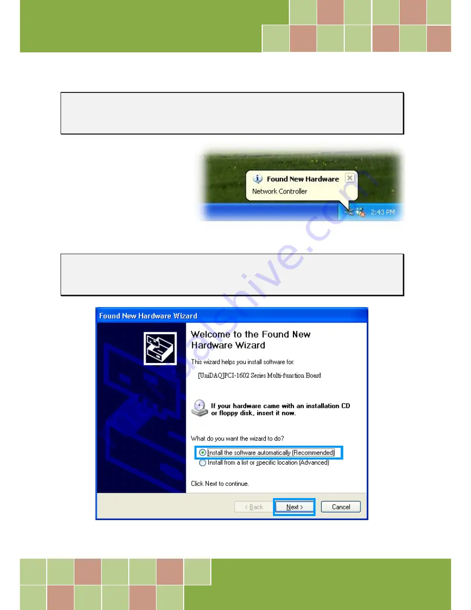
Step 2: Power on the computer and system should find the new card and then continue to 

finish the Plug&Play steps. 


Note:  Some  Windows  OS  will  load 
the 

driver 

automatically 

to 

complete the installation at boot.   


Step 3: Select 

“Install the software automatically *Reco” 

and click the 

“Next>” 

button. 


Summary of Contents for PCI-1202 Series

Page 1: ...ility for damages consequent to the use of this product ICP DAS reserves the right to change this manual at any time without notice The information furnished by ICP DAS is believed to be accurate and...

Page 2: ...2 2 JUMPER SETTING 21 2 2 1 JP1 A D Input Type Selection 21 2 2 2 J1 D A Reference Voltage Selection 22 2 2 3 D I Port Setting Pull High Low 22 2 3 CARD ID SWITCH 23 2 4 ANALOG INPUT SIGNAL CONNECTION...

Page 3: ...ERSION OPERATION 86 7 1 THE CONFIGURATION CODE TABLE 86 7 2 THE UNIPOLAR BIPOLAR 87 7 3 THE INPUT SIGNAL RANGE 87 7 4 THE SETTLING TIME 88 7 5 WHEN TO DELAY THE SETTLING TIME 88 7 6 THE AD CONVERSION...

Page 4: ...NDOWS 114 11 2 DIAGNOSTIC PROGRAM 117 11 2 1 Power on Plug Play Test 117 11 2 2 Driver Plug Play Test 117 11 2 3 D O Test 118 11 2 4 D A Test 118 11 2 5 A D Test 118 12 PERFORMANCE EVALUATION 119 APPE...

Page 5: ...printed Quick Start Guide One software utility CD One CA 4002 D Sub Connect Related Information Product Page http www icpdas com root product solutions pc_based_io_board pci pci 1202 html http www icp...

Page 6: ...Universal PCI PEX 1202H PCI Express 12 bit 2 ch 12 bit 32 S E 16 Diff 44 kS s 1 k PCI 1202HU Universal PCI PCI 1602U Universal PCI 12 bit 2 ch 16 bit 32 S E 16 Diff 100 kS s 8 k PCI 1602FU Universal P...

Page 7: ...modes for this series software trigger pacer trigger and external trigger each trigger mode uses MagicScan to perform the data acquisition The external trigger can be programmed to one of the three tr...

Page 8: ...eries card Digital Input Output 16 channels TTL compatible D I 16 channels TTL compatible D O High Speed data transfer rate refer to chapter 10 Analog Output 2 channels 12 bit DACs Bipolar voltage out...

Page 9: ...02 H HU A D converter 16 bit 200 k Samples Sec for PCI 1602 F FU A D converter 16 bit 100 k Samples Sec for PCI 1602 U Programmable input signal configuration Provides MagicScan function FIFO Size 1 k...

Page 10: ...0000 800 4 88 mV 0111 1111 1111 7FF 10 V 0000 0000 0000 000 16 bit ADC input voltages and output codes for PCI 1602 series 16 bit ADC Input Voltages and Output Codes Analog Input Digital Output Binary...

Page 11: ...1602 180x Series Card Multi Function Boards User Manual Ver 4 8 Mar 2015 PMH 0014 48 Page 11 1 2 The Block Diagram The block diagram of the PEX 1202 and PCI 1202 1602 1800 1802 series card is given as...

Page 12: ...nal 5 V TTL compatible Data Transfer Polling Accuracy 0 01 of FSR 1 LSB 25 C 10 V Zero Drift 4 ppm C of FSR Analog Output Channels 2 ch Resolution 12 bit Accuracy 0 06 of FSR 1 LSB 25 C 10 V Output Ra...

Page 13: ...t Yes 4 bit for Version 4 0 or above I O Connector Female DB37 x 1 Male 20 bit ribbon x 2 Dimensions L x W x D 162 mm x 100 mm x 22 mm 195 mm x 97 mm x 22 mm Power Consumption 300 mA 5 V Operating Tem...

Page 14: ...ammable pacer External 5 V TTL compatible Data Transfer Polling Accuracy 0 01 of FSR 1 LSB 25 C 10 V Zero Drift 2 ppm C of FSR Analog Output Channels 2 ch Resolution 12 bit Accuracy 0 06 of FSR 1 LSB...

Page 15: ...l Bus Type 3 3 V 5 V Universal PCI 32 bit 33 MHz 5 V PCI bus 32 bit 33 MHz Data Bus 16 bit Card ID Yes 4 bit No I O Connector Female DB37 x 1 Male 20 bit ribbon x 2 Dimensions L x W x D 188 mm x 105 m...

Page 16: ...dance 10 M 6 pF Trigger Modes Software Internal programmable pacer External 5 V TTL compatible Data Transfer Polling Accuracy 0 01 of FSR 1 LSB 25 C 10 V Zero Drift 2 ppm C of FSR Analog Output Channe...

Page 17: ...I 32 bit 33 MHz 5 V PCI bus 32 bit 33 MHz Data Bus 16 bit Card ID Yes 4 bit No Yes 4 bit No I O Connector Female DB37 x 1 Male 20 bit ribbon x 2 Dimensions L x W x D 200 mm x 105 mm x 22 mm Power Cons...

Page 18: ...VR1 VR101 VR2 VR3 VR100 J1 10V 5V ADC input 16 or 32 channels External Trigger Input Digital Input 16 channels Digital Output 16 channels JP1 1 2 5 6 PCI 1202 1800 1802 H L Board Layout OUT CON1 CON2...

Page 19: ...2 channels External Trigger Input Digital Input 16 channels Digital Output 16 channels JP1 1 2 5 6 VR201 VR202 VR203 SW1 1 2 3 4 JP2 3 1 2 Pull High Pull Low PEX 1202 H L Board Layout OUT CON1 CON2 PE...

Page 20: ...R2 VR4 J1 10V 5V DAC output 2 channels ADC input 32 channels External Trigger Input Digital Input 16 channels Digital Output 16 channels JP1 2 6 VR5 VR6 VR7 1 5 PCI 1602 U FU Board Layout OUT CON1 CON...

Page 21: ...input type For single ended inputs connect pin1 3 and pin2 4 For differential inputs pin3 5 and pin4 6 should be connected The configuration is illustrated in the figure below Single Ended Input 1 JP...

Page 22: ...nfiguration is illustrated in the figure below 10 Voltage Output 1 J1 3 2 Default Setting 5 Voltage Output 1 J1 3 2 2 2 3 D I Port Setting Pull High Low This DI ports can be pull high or pull low that...

Page 23: ...series cards in one computer The default Card ID is 0x0 For detail SW1 Card ID settings please refer to Table 2 1 Table 2 1 Default Settings OFF 1 ON 0 Card ID Hex 1 ID0 2 ID1 3 ID2 4 ID3 0x0 ON ON O...

Page 24: ...ure 2 4 5 connection is suitable for floating analog input signals Note In Figure 2 4 4 the maximum common mode voltage between the analog input source and the AGND is 70 Vp p so the user must take ca...

Page 25: ...age 25 Figure2 4 1 Differential input with grounded source Right way A D CH0 HI A D CH n HI A D CHn LO A GND n A D CH 0 LO Es 1 Es n S S PEX 1202 and PCI 1202 1602 1800 1802 series Figure2 4 2 Grounde...

Page 26: ...n LO to A GND at the computer CAUTION In Figure 2 4 4 the maximum common mode voltage between the analog input source and the AGND is 70 Vp p Make sure that the input signal is under specification fir...

Page 27: ...n 100 k 10 M 100 k 10 M PEX 1202 and PCI 1202 1602 1800 1802 series Figure 2 4 6 Connecting to a 4 20 mA Source A D CHn AGND R Shunt Resistor Example A 20 mA source current through a 125 resistor e g...

Page 28: ...r 4 8 Mar 2015 PMH 0014 48 Page 28 Signal Shielding Signal shielding connections in Figure 2 4 1 to Figure 2 4 6 are all the same Use a single point connection to frame ground not A GND or D GND Vin P...

Page 29: ...0x Series Card Multi Function Boards User Manual Ver 4 8 Mar 2015 PMH 0014 48 Page 29 2 5 Pin Assignments CON1 and CON2 Digital output and digital input connector for PEX 1202 and PCI 1202 1602 1800 1...

Page 30: ...PCI 1202 1602 180x Series Card Multi Function Boards User Manual Ver 4 8 Mar 2015 PMH 0014 48 Page 30 CON3 Single ended input pin assignment as follows...

Page 31: ...PCI 1202 1602 180x Series Card Multi Function Boards User Manual Ver 4 8 Mar 2015 PMH 0014 48 Page 31 CON3 Differential input pin assignment as follows...

Page 32: ...s to restart the computer To install your PEX 1202 and PCI 1202 1602 1800 1802 series card complete the following steps Step 1 Installing DAQ card driver on your computer first Step 2 Configuring Card...

Page 33: ...x Series Card Multi Function Boards User Manual Ver 4 8 Mar 2015 PMH 0014 48 Page 33 Step 3 Shut down and power off your computer Step 4 Remove all covers from the computer Step 5 Select an empty PCI...

Page 34: ...nction Boards User Manual Ver 4 8 Mar 2015 PMH 0014 48 Page 34 Step 6 Remove the PCI PCI Express slot cover form the PC Step 7 Remove the connector cover form the DAQ card Step 8 Carefully insert your...

Page 35: ...Step 9 Tighten the captive Phillips screw Step 10 Replace the computer cover Step 11 Power on the computer Confirm the PEX 1202 and PCI 1202 1602 1800 1802 series card is mounted on the motherboard Fo...

Page 36: ...ws you the detail steps to install these drivers The recommended installation procedure for Windows is given in Sections 4 1 to 4 3 4 1 Driver Installing Procedure Follow these steps Step 1 Run the co...

Page 37: ...nual Ver 4 8 Mar 2015 PMH 0014 48 Page 37 Step 3 Please install the appropriate driver for your OS 1 Click the item UniDAQ 2 Click the item DLL for Windows 2000 and XP 2003 Vista 32 bit 3 Double Click...

Page 38: ...demo program can be obtained from the following link and then click the Next button 10 Select No I will restart my computer later and then click the Finish button For detailed information about the U...

Page 39: ...e 39 Step 2 Power on the computer and system should find the new card and then continue to finish the Plug Play steps Note Some Windows OS will load the driver automatically to complete the installati...

Page 40: ...PCI 1202 1602 180x Series Card Multi Function Boards User Manual Ver 4 8 Mar 2015 PMH 0014 48 Page 40 Step 4 Click the Finish button Step 5 Windows pops up Found New Hardware dialog box again...

Page 41: ...and PCI 1202 1602 1800 1802 series card installed is correct on the computer as follows Step 1 Select the Start Control Panel and then double click the System icon on Windows Step 2 Click the Hardwar...

Page 42: ...1202 and PCI 1202 1602 1800 1802 series card well or not Before the self test you must complete the hardware and driver installation For detailed information about the hardware and driver installation...

Page 43: ...board One CA 3710 optional cable Provide a stable signal source for example dry battery 2 Connect a DN 37 to the CON3 3 Wire the signal source to A D channel_0 and then keep set the JP1 jumper to Sing...

Page 44: ...4 48 Page 44 The PCI 1800 Series Connect the AI_01 Pin01 to signal positive Connect the A GND Pin09 to signal negative 5 1 3 Analog Output Test Wiring 1 Prepare for device One DN 37 optional wiring te...

Page 45: ...jumper to 10 V voltage refer to Sec 2 2 2 and wire the signals as follows The PEX 1202 and PCI 1202 1602 1802 Series Connect the positive probe of Multi meter to D A_out0 Pin 18 Connect the negative p...

Page 46: ...tility exe will be placed in the default path after completing installation Default Path C ICPDAS UniDAQ Driver Double click the UniDAQUtility exe Note The PEX 1202L H software is fully compatible wit...

Page 47: ...4 8 Mar 2015 PMH 0014 48 Page 47 2 Get Digital Output Input Function test result Select the Port 0 Check channel 0 2 4 6 6 5 Click Digital Output item 4 Select the Port 0 8 The corresponding D I becom...

Page 48: ...Ver 4 8 Mar 2015 PMH 0014 48 Page 48 3 Get Analog Input Function test result Click Analog Input item 10 Click this button to start test 12 Confirm the configuration setting 11 Check analog input on C...

Page 49: ...he value read on meter may be a little difference from the DA value because of the resolution limit of meter or the measurement error Click Analog Output item 14 15 16 17 Select the Channel 0 Select t...

Page 50: ...wer on stage The fixed IDs for the PEX 1202 and PCI 1202 1602 1800 1802 series card are given as follows Table 6 1 PEX 1202 PCI 1202 Series Vendor ID 0x1234 Sub Vendor ID 0x0000 Device ID 0x5672 Sub D...

Page 51: ...C as shown in the following Figure6 1 Details of how to identify the PEX 1202 and PCI 1202 1602 1800 1802 series card of ICPDAS data acquisition boards based on the Sub vendor Sub device and Sub Aux I...

Page 52: ...it is designed for PCI 1602 series This function can be detecting how many PEX 1202 PCI 1202 1602 180x series cards in the system Also can be detect and save the I O resource information of every PEX...

Page 53: ...nd the board number is to use DEMO15 EXE given in DOS demo program This demo program will send to D O and read back from D I If the user installs a 20 pin flat cable between CON1 and CON2 the value re...

Page 54: ...ter R W 32 bit 3Ch or 3Eh 3Fh On board NV RAM access control register R W 32 bit 8 bit 6 4 1 00h 8254 timer0 R W 8 16 32 bit 04h 8254 timer1 R W 8 16 32 bit 08h 8254 timer2 R W 8 16 32 bit 0Ch 8254 co...

Page 55: ...icrosystem Components Handbook for 8254 programming The block diagram of the 8254 timer is given as follows Figure 6 4 1 The Block diagram of 8254 timer for the PEX 1202 PCI 1202 1602 180x series CLK...

Page 56: ...xff void disable_timer0 void outport WORD wAddrTimer 3 4 0x34 disable pacer timer_0 outport WORD wAddrTimer 0 4 0x01 outport WORD wAddrTimer 0 4 0x00 timer1 for External Trigger void enable_timer1 WOR...

Page 57: ...r 3 4 input clock 8 M down count 8 time 1 s down count 65536 8 8192 s max 8191 s WORD P180X_DelayUs WORD wDelayUs WORD wDownCount wLow wHigh wVal double fTimeOut if wDelayUs 8191 return InvalidateDela...

Page 58: ...of trigger register wAddrCtrl 1 4 Figure 6 5 1 The flow path of analog input signal MUX AMP1 ADC Max 10V Max 5V Signals Single ended Differential AMP1 0 1 0 1 Gain Rang 4 3 2 1 0 7 6 9 8 6 5 1 The Con...

Page 59: ...202 1602 1800 1802 16 1 0 0 0 0 1202 1602 1802 31 1 1 1 1 1 1202 1602 1802 6 5 1 2 Bit6 Bit7 Bit8 Bit9 Configuration Table Bit6 Bit7 Gain Control B7 B6 Low Gain High Gain 0 0 PGA 1 PGA 1 0 1 PGA 2 PGA...

Page 60: ...5 V 4 3 s 0111 Unipolar 0 V 10 V 1 3 s 1000 Unipolar 0 V 5 V 2 3 s 1001 Unipolar 0 V 2 5 V 4 3 s 1010 Unipolar 0 V 1 25 V 8 3 s 1011 The configuration table of PEX 1202H and PCI 1202 1800 1802 H HU is...

Page 61: ...1602 series WORD P180X_SetChannelConfig WORD wAdChannel WORD wAdConfig WORD wConfig wChannel wChannel wAdChannel 0x1f wSysConfig wAdConfig 0x1f store for P1802_AdPolling wConfig wAdConfig 0x0f wConfi...

Page 62: ...break case 9 wZERO 0 dfMAX 5 0 2 0 break case 10 wZERO 0 dfMAX 2 5 2 0 break case 11 wZERO 0 dfMAX 1 25 2 0 break case 0x10 wZERO 2048 dfMAX 5 0 break case 0x11 wZERO 2048 dfMAX 0 5 break case 0x12 w...

Page 63: ...st 48 scan channels can be stored in the MagicScan controller Start MagicScan 1 0 1 Start the MagicScan controller Stop MagicScan 0 1 0 Stop the MagicScan controller Get ODM number 1 1 0 Get the ODM n...

Page 64: ...rt wAddrCtrl 0x04 0 outport wAddrCtrl 0xffff send a recovery to PIC j 0 while inport wAddrCtrl 0x04 0 j if j 65530 return AdControllerError time out i i 0xDFFF set pic low outport wAddrCtrl i j 0 whil...

Page 65: ...WORD P180X_SetChannelConfig WORD wAdChannel WORD wAdConfig WORD wConfig wChannel wChannel wAdChannel 0x1f wSysConfig wAdConfig 0x1f store for P1802_AdPolling wConfig wAdConfig 0x0f wConfig wConfig 6 w...

Page 66: ...AlarmTypeError wMagicLowAlarm wMP wLowAlarm wMagicHighAlarm wMP wHighAlarm wMagicAlarmType wMP wAlarmType wChannel wAdChannel 0x1f wMagicChannel wMP wChannel wSysConfig wAdConfig 0x1f Store for P180X...

Page 67: ...180X_StartScan WORD wSampleRate WORD wNum WORD wVal WORD wRetVal wMagicNum wNum disable_timer0 Disable pacer timer first start MagicScan controller wRetVal pic_control 0xD400 11 1 01 cmd_101 start sca...

Page 68: ...formed by software The operation steps of middle trigger are given as follows Step 1 Disable all external trigger Step 2 Set the pacer rate of timer 1 Step 3 Clear FIFO enable timer 1 Step 4 Circular...

Page 69: ...arScan P180X_AddToScan P180X_SaveScan P180X_AddToScan P180X_AddToScan P180X_StartScanPostTrg Or P180X_StartScanPreTrg Or P180X_StartScanMiddleTrg P180X_WaitMagicScanFinish Perform Aanlysis P180X_SaveS...

Page 70: ...pleRateDiv DATALENGTH nPriority if wRetVal 0 sprintf cShow 2 External Post Trigger Setup OK else sprintf cShow 2 External Post Trigger Setup Error TextOut hdc x dx y iLine dy cShow strlen cShow iLine...

Page 71: ...and enable timer 1 4 waiting for the external signal to stop timer 1 5 circular fetch the last N data 6 stop all timer and disable all trigger Middle trigger for PEX 1202 and PCI 1202 1602 180x ver F...

Page 72: ...1 01 cmd_101 start scan if wVal 0 return wVal _outpw wAddrCtrl 0xf000 1 disable all external trigger enable_timer1 wSampleRateDiv 2 Sampling rate 8M dwSampleRateDiv _outpw wAddrCtrl 0x7000 3 B15 0 S2...

Page 73: ...n if wVal 0 return wVal _outpw wAddrCtrl 0xf000 1 disable all external trigger enable_timer1 wSampleRateDiv 2 Sampling rate 8M dwSampleRateDiv _outpw wAddrCtrl 0x6800 3 B15 0 S2 0 S1 1 S0 0 clr FIFO _...

Page 74: ...1 start scan if wVal 0 return wVal _outpw wAddrCtrl 0xf000 1 disable all external trigger enable_timer1 wSampleRateDiv 2 Sampling rate 8M dwSampleRateDiv _outpw wAddrCtrl 0x6800 3 B15 0 S2 0 S1 1 S0 0...

Page 75: ...f000 1 disable all external trigger enable_timer1 wSampleRateDiv 2 Sampling rate 8M dwSampleRateDiv _outpw wAddrCtrl 0x6800 3 B15 0 S2 0 S1 1 S0 0 clr FIFO _outpw wAddrCtrl 0xE800 3 B15 1 S2 0 S1 1 S0...

Page 76: ...xf000 1 disable all external trigger enable_timer1 wSampleRateDiv 2 Sampling rate 8M dwSampleRateDiv _outpw wAddrCtrl 0x6800 3 B15 0 S2 0 S1 1 S0 0 clr FIFO _outpw wAddrCtrl 0xE800 3 B15 1 S2 0 S1 1 S...

Page 77: ...tScanPostTrg demo23 c for PEX 1202 PCI 1202 P1202_StartScanPreTrg demo24 c for PEX 1202 PCI 1202 P1202_StartScanMiddleTrg demo25 c for PEX 1202 PCI 1202 P1602_StartScanPostTrg demo23 c for PCI 1602 P1...

Page 78: ...WORD j if inport wAddrCtrl 0x04 0 outport wAddrCtrl 0xffff send a recovery to PIC j 0 while inport wAddrCtrl 0x04 0 j if j 65530 return AdControllerError time out i i 0xDFFF set pic low outport wAddr...

Page 79: ...2 Handshake signal between host PC and MagicScan controller Bit5 FIFO Empty 0 FIFO is Empty Bit4 ADC Busy 0 ADC is Busy Bit1 ODM indicator non ODM version 0 ODM version ODM bit string Bit7 FIFO Half F...

Page 80: ...gned for PCI 1800 1802 series P1202_AdPollingHex is designed for PEX 1202 PCI 1202 series P1602_AdPollingHex is designed for PCI 1602 series WORD P180X_AdPollingHex Word AdVal WORD wVal wTime Clear FI...

Page 81: ...channel digital input and 16 channel digital output All levels of DI DO are TTL compatible The connections diagram and block diagram are given below Figure 6 6 1 1 DIO Block Diagram The D I port can...

Page 82: ...rt wAddrDio 0xffff return NoError WORD P180X_Do WORD wDo outport wAddrDio wDo return NoError 6 6 2 Card ID Register Read wAddrDIO 0x4h Bit 7 Bit 6 Bit 5 Bit 4 Bit 3 Bit 2 Bit 1 Bit 0 0 0 0 0 ID3 ID2 I...

Page 83: ...ad Write BAR4 0 A D FIFO DAC1 write BAR4 4 Reserved DAC2 write The PEX 1202 and PCI 1202 1602 1800 1802 series card provides 2 independent 12 bits D A converters with double buffer bipolar voltage out...

Page 84: ...ature of PEX 1202 and PCI 1202 1602 1800 1802 series The sample code for D A is given as follows P180x_Da is designed for PCI 1800 1802 series P1202_Da is designed for PEX 1202 PCI 1202 series P1602_D...

Page 85: ...0X_AdPollingHex Word AdVal WORD wVal wTime Clear FIFO outport wAddrCtrl 0x2000 B15 0 clear FIFO B13 1 not MagicScan controller cmd outport wAddrCtrl 0xA000 B15 1 no clear FIFO B13 1 not MagicScan cont...

Page 86: ...r 2 5 V 2 3 s 0x06 Bipolar 1 25 V 4 3 s 0x07 Unipolar 0 V 10 V 1 3 s 0x08 Unipolar 0 V 5 V 2 3 s 0x09 Unipolar 0 V 2 5 V 4 3 s 0x0A Unipolar 0 V 1 25 V 8 3 s 0x0B PEX 1202 H and PCI 1202 1800 1802 H H...

Page 87: ...x0 Bipolar 5 V 2 5 s 0x1 Bipolar 2 5 V 4 5 s 0x2 Bipolar 1 25 V 8 5 s 0x3 7 2 The Unipolar Bipolar If the analog input signal is unipolar you can measure this signal with bipolar setting this will red...

Page 88: ...Scan controller will change the channel number and gain control just after every pacer trigger signal Therefore the limitation is settling time pacer timer in MagicScan mode 7 5 When to Delay the Sett...

Page 89: ...PCI 1600 series The functions of fixed channel mode are given as follows 1 P180x_SetChannelConfig The reading data is in floating format 2 P180x_AdPolling 3 P180x_AdsPolling 4 P180x_AdsPacer The func...

Page 90: ..._FunA_Get The functions of continuous capture with storing data to main memory are given as follows single board operating 1 P180x_FunB_Start 2 P180x_FunB_ReadStatus 3 P180x_FunB_Stop 4 P180x_FunB_Get...

Page 91: ...aveScan Select the active channel 1 Delay for the settling time if needed Analyses the AD data 1 Delay for the settling time if needed Perform one AD conversion Analyses the AD data 2 Select the activ...

Page 92: ...nnel number in the scan list can be random and duplicated The AD data of MagicScan can be saved in array if P180X_SaveScan is used The flowchart is given as follows P180X_ClearScan P180X_AddToScan P18...

Page 93: ...n sequence control The scan sequence is one by one and repeatable with the limitation of maximum 48 channels So the following scan sequence is all valid One Channel MagicScan 0 Two Channels MagicScan...

Page 94: ...ng rate between channels the digital filter will be active at the same time This is a situation of ALL or NO You can use both the digital filter and the different sampling rate at the same time or use...

Page 95: ...5 The MagicScan Function The features of MagicScan are given as follows 1 Different gain for each channel 2 Non sequential order for channel scan 3 Different sampling rate for each channel use with di...

Page 96: ...a will be placed in the FIFO 4 PC will read the A D data from FIFO while the data is ready The FIFO is 1 k samples for PCI 1800 and 8 k samples for PCI 1802 The PC can will compute and analyze the A D...

Page 97: ...he software averages the continue two 2 into one 2 to get 55 k as follows 2 2 2 2 2 2 2 2 2 2 2 2 55 k The software has to fetch the 3 3 3 3 3 in 11 k therefore the software average the continue ten 3...

Page 98: ...cSum j 0 for j 0 j wMP j wMagicNow j wMagicAve j for j 0 j wMP j wMagicP j 0 for i 0 i wMP i skip the MagicScan settling time dwTime 0 for wVal inport wAddrCtrl 0x20 if wVal 0 break dwTime if dwTime 1...

Page 99: ...2 low alarm if wVal wMagicLowAlarm j dwMagicLowAlarm dwIndex else if w3 1 1 high alarm if wVal wMagicHighAlarm j dwMagicHighAlarm dwIndex else if w3 4 4 high or low alarm if wVal wMagicLowAlarm j dwMa...

Page 100: ...unctions provided by PEX 1202 and PCI 1202 1602 1800 1802 series card can send out the user defined arbitrary waveform by software and perform the A D conversion by hardware at the same time The M_Fun...

Page 101: ...channels max 2 Perform MagicScan A D conversion by hardware at the same time 32 channels max 3 Only one function call is needed 4 Very easy to use The driver can send out the D A wave form output to...

Page 102: ...i task OS If the user want to generate the periodic wave form such as sine cosine the M_Functions can provide the output wave form over 100 k Samples sec The 5 V 100 kS s sine wave shown in Figure 8 3...

Page 103: ...A D input channels are programmable The comparison table is given as follows Driver Name D A A D P180X_M_FUN_1 Channel_0 sine wave channel_0 10V P180X_M_FUN_2 Channel_0 arbitrary wave form channel_0 1...

Page 104: ...D A output waveform will be distorted sometimes Refer to Figure 8 5 for details If the user has to generate the periodic wave form such as sine cosine and the analysis is similar to spectrum analysis...

Page 105: ...these three applications The software driver can support 16 cards max in one PC system The software also supports 2 cards for continuous capture function The continuous capture functions are specially...

Page 106: ...ntinuous capture The P180X_Card _StartScan will perform the following function 1 setup scan queue 2 setup channel gain data 3 setup continuous capture data 4 create a multi task thread for long time d...

Page 107: ...setup continuous capture function this function will create thread if wRet NoError Show error message return now the thread is active and the continuous capture function is going now for wRetVal P180...

Page 108: ...rtScan setup continuous capture function this function will create thread if wRet NoError Show error message return now the thread is active and the continuous capture function is going now for wRetVa...

Page 109: ...first then analyze these data later memory size 330 k 60 2 5 330 k 150 49 5 M word 99 M bytes Refer to demo22 c for 330 k 2 5 minutes continuous capture using 99 M bytes of the PC memory The P180X_Fu...

Page 110: ...PCI 1202 1800 1802 H HU Step 5 Run DEMO19 EXE Step 6 Adjust VR101 until CAL_0 7FF or 800 Step 7 Adjust VR100 until CAL_1 FFE or FFF Step 8 Repeat Step6 Step7 until all OK Step 9 Adjust VR1 until CAL_...

Page 111: ...6250 V POWER On OFF ICP DAS Output Vlotage OUT CON3 CON2 PCI 1602 1602F REV 1 0 IN CON1 VR1 VR3 VR2 VR4 J1 10V 5V JP1 2 6 VR5 VR6 VR7 1 5 CH 0 CH 1 CH 2 CH 16 A GND DN 37 I O CONNECTOR BLOCK Figure 1...

Page 112: ...age meter 0 V Step 10 Send 0 to D A channel 1 Step 11 Adjust VR203 until voltage meter 10 V For PCI 1800 1802 version_C series card Step 1 J1 select 10 V Step 2 Connect the D A channel 0 to voltage me...

Page 113: ...N2 PCI 1602 1602F REV 1 0 IN CON1 VR1 VR3 VR2 VR4 J1 10V 5V JP1 2 6 VR5 VR6 VR7 1 5 CH 17 DAC output channel 0 DN 37 I O CONNECTOR BLOCK CH 16 A GND Figure 10 2 D A Calibration Note 1 The CH 18 36 are...

Page 114: ...r files for different development environments will be presented as follows Demo Program for PCI 1202 1602 180x Series Classic Driver The demo program of PEX 1202 and PCI 1202 series is contained in C...

Page 115: ...demo scan sequence 1 2 0 demo18 one board MagicScan demo scan 32 channel show channel 0 1 15 16 17 demo19 one board A D calibration demo20 two board P180X_FUNA continuous capture demo demo21 single bo...

Page 116: ...os pci unidaq dll demo There are about demo program given as follows Analog Input Pacer Analog Input Pacer Continue Analog Input Pacer Scan Analog Input Pacer Scan Continue Analog Input Pacer Scan EXT...

Page 117: ...er_ID 1234 device_ID 5672 PEX PCI 1202 If the plug play ROM BIOS can detect the PEX 1202 and PCI 1202 1602 1800 1802 series in the power on time the software driver of DOS Windows 95 98 NT 2000 will f...

Page 118: ...602 1800 1802 card with DA channel 0 connected to A D channel 0 Step 3 Power on PC run DEMO1 EXE Step 4 Check the value of A_0 1 25 volt Step 5 Run DEMO5 EXE Step 6 Check the wave form shown in screen...

Page 119: ...ion one card two channels Total 20 kS s 10 kS s per channels DEMO14 EXE 20 kS s Continuous capture function two card two channels Total 20 kS s 10 kS s per channels DEMO5 EXE 20 k sine max M_function...

Page 120: ...pin DN 37 The DN 37 is a general purpose daughter board for DB 37 pins with DIN Rail Mountings They are also designed for easy wire connection via pin to pin A2 DB 8125 The DB 8125 is a daughter boar...

Page 121: ...d Input Board The DB 16P is a 16 channel isolated digital input daughter board The optically isolated inputs of the DB 16P are consisted of are bi directional optocoupler with resistor for current sen...

Page 122: ...al type terminal block The relay is energized by applying 5 voltage signal to the appropriate relay channel on the 20 pin flat connector There are 16 enunciator LEDs for each relay light when their as...

Page 123: ...flat cable connector only 16 relays are used or 50 pin flat cable connector OPTO 22 compatible for DIO 24 series Twenty four enunciator LEDs one for each relay light when their associated relay is ac...

Reviews: