Chapter 2. Architecture and technical overview
37
Draft Document for Review October 14, 2014 10:19 am
5137ch02.fm
2.2.1 POWER8 processor overview
The POWER8 processor is manufactured using the IBM 22 nm Silicon-On-Insulator (SOI)
technology. Each chip is 649 mm
2
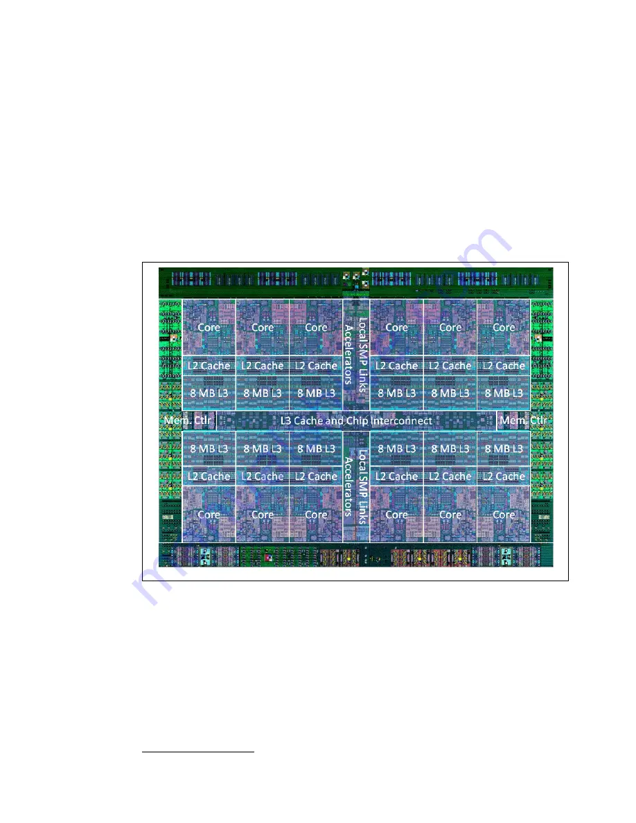
and contains 4.2 billion transistors. As shown in Figure 2-6,
the chip contains 12 cores, two memory controllers, PCIe Gen3 I/O controllers, and an
interconnection system that connects all components within the chip. On some systems only
6, 8, 10, or 12 cores per processor may be available to the server. Each core has 512 KB of
L2 cache, and all cores share 96 MB of L3 embedded DRAM (eDRAM). The interconnect
also extends through module and board technology to other POWER8 processors in addition
to DDR3 memory and various I/O devices.
POWER8 systems use memory buffer chips to interface between the POWER8 processor
and DDR3 or DDR4 memory
1
. Each buffer chip also includes an L4 cache to reduce the
latency of local memory accesses.
Figure 2-6 The POWER8 processor chip
The POWER8 processor is for system offerings from single-socket servers to multi-socket
Enterprise servers. It incorporates a triple-scope broadcast coherence protocol over local and
global SMP links to provide superior scaling attributes. Multiple-scope coherence protocols
reduce the amount of SMP link bandwidth that is required by attempting operations on a
limited scope (single chip or multi-chip group) when possible. If the operation cannot
complete coherently, the operation is reissued using a larger scope to complete the operation.
1
At the time of the publication, the available POWER8 processor-based systems use DDR3 memory.


