


Rev. 1.00
16� of ���
�an�a�� 1�� �01�
Standard 8051 8-Bit Flash MCU
HT85F2260/HT85F2270/HT85F2280
Analog to Digital Converter –
ADC
Programming Considerations
During microcontroller operations where the A/D converter is not being used, the A/D internal
circuitry can be switched off to reduce power consumption, by setting bit ADOFF high in the
ADCR0 register. When this happens, the internal A/D converter circuits will not consume power
irrespective of what analog voltage is applied to their input lines. If the A/D converter input lines
are used as normal I/Os, then care must be taken as if the input voltage is not at a valid logic level,
then this may lead to some increase in power consumption.
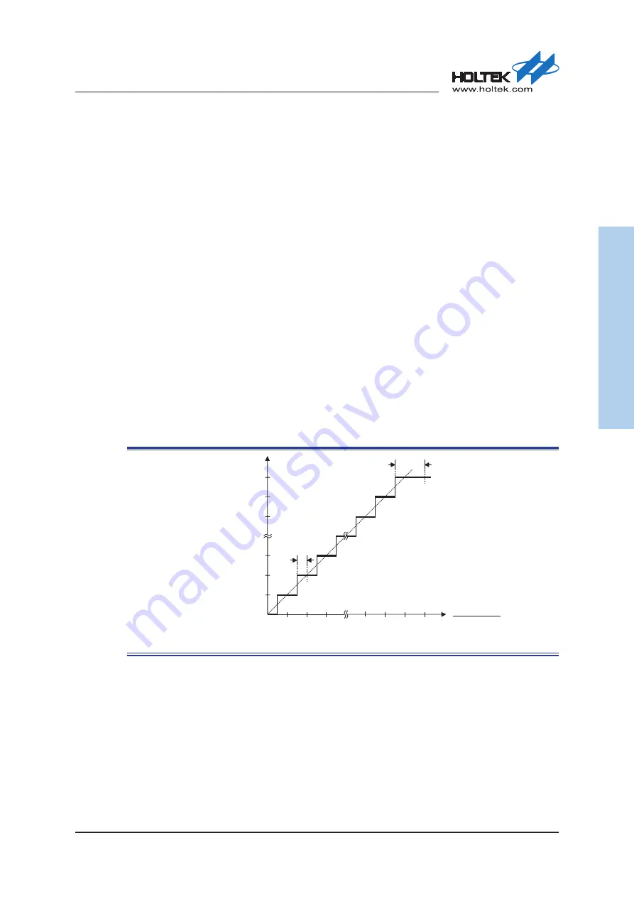
A/D Transfer Function
As the converted data is 12-bit wide, its full-scale converted digitised value is equal to FFFH.
Since the full-scale analog input value is equal to the VCCA3 or V
REF
voltage, this gives a single bit
analog input value of VCCA3 or V
REF
divided by 4096.
1 LSB=(VCCA3 or V
REF
)/4096
The A/D Converter input voltage value can be calculated using the following equation:
A/D input voltage=PGA Gain×A/D digital value×(VCCA3 or V
REF
)/4096
The diagram shows the ideal transfer function between the analog input value and the digitised
output value for the A/D converter. Except for the digitised zero value, the subsequent digitised
values will change at a point 0.5 LSB below where they would change without the offset, and the
last full scale digitised value will change at a point 1.5 LSB below the VCCA3 or V
REF
level.
Ideal A/D Transfer Function (PGA=1)