background image

48

42PD9700C/U & 55PD9700C/U

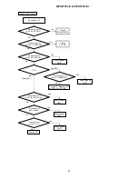
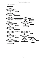
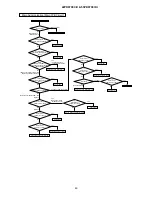
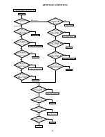
Sub Picture [Main P

C

B Circuit]

Check FC P

C

B

No

No

Yes

Yes

Yes

Are waveform at 

TP608(Y), TP609(Cb), and 

TP610(Cr)?

Are waveforms at 

42pin(Y), 44pin(Cb), and 

46pin(Cr) of I601?

RGB

Input(DTT,SCART) or  Compo-

nent Input?

Are waveforms at 

78pin(Y), 80pin(Cb), and 

2pin(Cr) of I601?

Are waveforms at 

21pin(Y), 22pin(Cb), and 

23pin(Cr) of I504?

Are waveforms at 

56pin(Y) and 58pin(C) of  I201?

Are waveforms at 

44pin(Y) and 43pin(C) of  I504?

Is

waveform at 1pin(CV) of 

I504?

Is

waveform at 53pin(CV) 

of  I201?

Is

waveform at 63pin(CV) of

I201?

Check Q604, Q605, Q606

Check I601

Yes

Check I504

Yes

Check I201

Check U101

Yes

Check Q206 and Q511

Yes

Yes

Check Q515, Q516, Q517

Yes

No

(RF/Composit

  Video/S-Video)

No

No

RF or Composit Video ?

No

Yes

(RF or Composit Video)

No

(S-Video)

Check I504

Check Q512, Q513

No

No

No

No

Check I201 and Input terminal

Check I201 and Input terminal

RF Input?

Yes (RF)

No

(Composit Video)

Trouble of Sub picture

SCART

or

Component?

No

(DTT)

No

Yes(SCART,Comp)

Check I601

and Input terminal

Yes

Check around I601 

Check DTT Module, U101

and P702 on FC P

C

B

Are waveform at 

2pin(R), 4pin(G), 6pin(B) of 

PMD1?

Yes

(RGB(DTT,SCART) or Component

 Video except 480i and 576i)

Summary of Contents for 42PD9700C

Page 1: ...oduktsicherheit in diesem Wartungshandbuch zu lesen SERVICE MANUAL MANUEL D ENTRETIEN WARTUNGSHANDBUCH Data contained within this Service manual is subject to alteration for improvement Les données fournies dans le présent manuel d entretien peuvent faire l objet de modifications en vue de perfectionner le produit Die in diesem Wartungshandbuch enthaltenen Spezifikationen können sich zwecks Verbes...

Page 2: ...oltage part and power supply part Possible to die if you tough to these place by miss take Please disconnect power plug during overhaul reassemble or change parts You will die or take damage by electric shock if you touch to live part Use recommended components Please use to same characteristic com ponent which is same as previous for your safety and keep reliability espe cially marked by in parts...

Page 3: ... inch colour plasma display panel with a resolution of 1024 H x 1080 V pixels creates a high definition large screen aspect ratio 16 9 and low profile flat display Free from electromagnetic interferences from geo magnetic sources and ambient power lines the panel produces high quality display images free from color mis convergence and display distortion High Performance Digital Processor A wide ra...

Page 4: ...42 55PD9700U and 42 55PD9700C according to country This logo indicates that the product is compliant with European Digital Broadcasting DVB is a registered trademark of the DVB Project This logo indicates that the product is set up to view digital terrestrial TV FREEVIEW and the FREEVIEW logo are trade marks of DVT Services Ltd and are used under license FREEVIEW Logo DTV Services Ltd 2002 This lo...

Page 5: ...ut terminal RCA S video input terminal Mini DIN L R audio input terminal RCA HDMI 1 2 HDMI input terminal Audio input terminal 3 5mm Stereo Mini Jack Photo Input Photo Input terminal SD card slot Input signals Composite video PAL SECAM NTSC3 58 NTSC4 43 PAL60 Component video 480i 576i 480p 576p 720p 50 720p 60 1080i 50 1080i 60 Output Signal OUTPUT MONITOR composite video monitor output terminal R...

Page 6: ...roughly after the lead free solder has been completely melted do not apply the soldering iron without solder Servicing soldering iron A soldering iron with a temperature setting capability temperature control function is recommended The melting point of lead free solder is higher than leaded solder Use a soldering iron that maintains a high stable temperature large heat capacity and that allows te...

Page 7: ...ectly Freeze Multi Mode Hold Press this button to change the picture to freeze mode Press it again to return to normal picture In addition during multi picture mode each time press this button the picture is changed to 2 4 and 12 multi mode Also it holds the page in text mode Colour Red Green Yellow Blue Index Time Cancel Pressing this button can indicate the time by On Screen display when receivi...

Page 8: ...5V PULL UP 23 RMCON I O PDP Receiving Remote Control Signal 24 NC I O PDP NC 25 V FREQ_3 I O PDP V Frequency 26 SCV SYNC I O PDP SUB_Y SYNC Composite 27 IRQ PM IRQ I O PDP PDP Control 28 MCV SYNC I O PDP MAIN_Y SYNC Composite 29 POWER_LED I O PDP L Lighting Power Save 30 FUNC_2 I O PDP EXT CONT 2 Function2 EXTernal Control 2 31 CEC_OUT I O PDP CEC OUT CEC1 32 H FREQ_3 I O PDP H Frequency 33 PDWN I...

Page 9: ...W 76 ASEL2 I O PDP Audio Switching SW 77 SDA2 I O PDP I2C TAS3103 TAS5508 78 SCL2 I O PDP I2C TAS3103 TAS5508 79 D SUB COMP_SYNC SW I O PDP D SUB COMP for Sync Switching 80 BM_SW I O BM Switching 81 RGB_BLK_2 I O RGB Blank 2 82 RGB_BLK_3 I O RGB Blank 3 83 AUDIO_RESET I O Audio Circuit Reset 84 PDP_WVGA_LCD_SW_1 I O PDP 42WVGA LCD Detection 85 5 0V I 86 EDID_PROTECT_1 I O PDP Memory Protect Not ne...

Page 10: ...3 DTT_POWER I O PDP DTT POWER 114 DISPEN I O PDP DISPEN Backlight on 115 HDMI_A_SW I O PDP HDMI AUDIO SW 116 SCL5 I O PDP I2C Sil9021 117 SDA5 I O PDP I2C Sil9021 118 SCL6 I O PDP I2C To the Side of Sensor Board AD7414 119 SDA6 I O PDP I2C To the Side of Sensor Board AD7414 120 COLOR_SYS I O PDP Color System Pull in range Switching 121 AD_KEY3 I O PDP AD KEY3 122 AD_KEY2 I O PDP AD KEY2 123 AD_KEY...

Page 11: ... DET_1 SW_L_OUT SW_L_OUT RXD2 DISPEN EXT_RESET PDP_WVGA_LCD_SW2 PDP_WVGA_LCD_SW1 HDMI_HPD_RESET P120 P17 SOUT3 CLK3 P113 P61 P60 TXD2 P55 P50 CNVss RXD1 TXD1 P64 P65 P112 CLK4 AN25 P130 P131 AN26 AN27 P02 SIN3 P125 P126 P127 P122 P123 P124 P134 P137 P03 SOUT4 P07 P47 P97 P46 P53 AN6 TA3IN TA4IN P133 P33 P32 P115 P04 P06 P110 P111 P100 P54 P10 P11 P132 P75 P51 P52 RXD0 TXD0 P102 P141 P107 P05 P15 P...

Page 12: ...ory Initialize operation NOTE The execution of this function returns the adjustment codes to the preset values therefore adjust ment data will be lost Procedure 1 Enter Adjustment Mode 2 Select MEMORY INIT adjustment code No 898 and change the data value from 0 to 1 3 Activate MEMORY INIT by pressing OK button 4 Select No 712 and change data value from 1 to 0 5 Check that the receiving channel goe...

Page 13: ...nput Level VIDEO 7 7 FC 27YNR Input Level Scart RGB 50 60Hz 7 7 FC 28YNR Input Level 480i 576i 7 7 FC 29YNR Input Level 480p 576p 7 7 FC 30YNR Input Level for AV1 5 Mode 1080i 50 60 720p 7 7 FC 31YNR Input Level for HDMI Mode 480i 480p 576i 576p VGA 7 7 FC 32YNR Input Level for HDMI Mode 1080i 50 60 720p 7 7 FC 33CNR Input Level at Low level for AV1 5 Mode RF VIDEO 7 3 FC 34CNR Input Level at Low ...

Page 14: ...128 FC 82B Y Clamp Offset HDMI 1080i 50 60 255 128 FC 83R Y Clamp Offset HDMI 1080i 50 60 255 128 FC 84B Y Clamp Offset HDMI 720p 255 128 FC 85R Y Clamp Offset HDMI 720p 255 128 FC 86FC6 THROUGH 0 OFF 1 THROUGH ON 1 0 FC 87Dynamic Back Light Correction For LCD 1 1 FC 88Dynamic Contrast Correction 1 1 FC 89Histogram Color Management 1 1 FC 90Histogram Gradation Amp 1 1 FC 91Histogram Enhancer 1 1 F...

Page 15: ...TSC4 43 Sub 10 7 TB1274 144Y_DL 6 0SECAM Sub 10 5 TB1274 145Y_DL 6 5PAL NTSC4 43 Sub 10 5 TB1274 146Y_DL 6 5SECAM Sub 10 5 TB1274 147Y_DL L Sub 10 5 TB1274 148Y_DL L Sub 10 5 TB1274 149Y_DL VIDEO PAL NTSC4 43 Sub 10 5 TB1274 150Y_DL VIDEO SECAM Sub 10 5 TB1274 151Y_DL VIDEO NTSC Sub 10 5 TB1274 152NTSC Comb Comb off Sub 1 1 TB1274 153Cb offset1 Sub 15 8 TB1274 154Cr offset1 Sub 15 8 TB1274 155MVM ...

Page 16: ...205V_SEP 1 1080i_50 1 0 TA1391FG 206V_SEP 1 1080i_60 720p 1 0 TA1391FG 207V_SEP 2 RF VIDEO 1 0 TA1391FG 208V_SEP 2 480i 576i 1 0 TA1391FG 209V_SEP 2 480p 576p 1 0 TA1391FG 210V_SEP 2 1080i_50 1 0 TA1391FG 211V_SEP 2 1080i_60 720p 1 0 TA1391FG 212AFC MODE 1 RF 3 0 TA1391FG 213AFC MODE 1 VIDEO 3 0 TA1391FG 214AFC MODE 2 RF 3 0 TA1391FG 215AFC MODE 2 VIDEO 3 0 TA1391FG 216N_LVL 1 RF 1 0 TA1391FG 217N...

Page 17: ...z Cinema mode 3 3 PDP 261Q mode 0 Freeze 1 Move 1 2 Move 2 3 Movie3 For 70Hz PC 3 0 PDP 262Sub Contrast 1 15kHz System 15 4 TA1391FG 263Vak OFfSet Vak_OFS 255 0 PDP 264Vak to Vra Parameter VaktoVra 255 1 PDP 265Vsk to Vrs Parameter VsktoVrs 255 1 PDP 266VFB WAIT CounTer CT_VWAIT 255 60 PDP 267VFB CORRection Counter CT_VCORR 255 15 PDP 268Vsk OFFSet Vsk_OFS 255 0 PDP 269Uvrs Uvra RECALL RCLVr 1 0 P...

Page 18: ...A5361 326TEXT V sync delay 127 50 SAA5361 327TEXT_H_POSITION 254 48 SAA5361 328TEXT_V_POSITION 254 39 SAA5361 329Select for APC output Except Europe model Main RF 2 1 SAA5361 330L_PLL GAIN 1 0 TDA9885 331HDMI EDID WRITE ENABLE s 1 0 M30627 332 HDMI Ccolorimetry Judgement 0 Signal Format Priority 1 AVI InfoFrame Priority HDMI 1 0 HDMI 333BPMA Back Porch Mode Field2 Position Adjustment 1 1 HDMI 334T...

Page 19: ...ion Mode YCSV 1 0 3 0 uPD64015 3893 Line Comb Select Sensitivity Setting1 VCOMA 1 0 3 2 uPD64015 3903 Line Comb Select Sensitivity Setting2 VCOMB 1 0 3 2 uPD64015 391Y Trap Filter Characteristic Select NTSC PAL YCSHY 1 0 3 0 uPD64015 392C Separate Filter Characteristic Select NTSC PAL YCSHC 1 0 3 0 uPD64015 393Chroma Output Filter Processing Select COBPFOFF 1 0 uPD64015 394 Chroma Output Frequency...

Page 20: ...etting YNRMDOFF 1 1 uPD64015 442CNR Process Stop CNRSTOP 1 1 uPD64015 443CNRLPF Process Yes No CNRLPFON 1 0 uPD64015 444CNR Nonlinear Filter Gain Setting CNRGAIN 1 0 3 3 uPD64015 445CNR Nonlinear Filter Convergence Level Setting CNRCORE 2 0 7 3 uPD64015 446CNR Nonlinear Filter Limit Level Setting CNRLIM 2 0 7 3 uPD64015 447CNR Motion Detection between Frames Coring Setting CMVDCORE 3 0 15 4 uPD640...

Page 21: ...LTICORE 3 0 NTSC 11 3 uPD64015 506 Except NTSC 11 3 uPD64015 507 480i 576i 11 3 uPD64015 508Filter Setting for CTI CTITAP 2 0 RF M 7 2 uPD64015 509 RF Except M 7 2 uPD64015 510 NTSC 7 2 uPD64015 511 Except NTSC 7 5 uPD64015 512 480i 576i 7 2 uPD64015 513Coring Setting for CTI CTICORE 3 0 RF M 9 3 uPD64015 514 RF Except M 9 3 uPD64015 515 NTSC 9 3 uPD64015 516 Except NTSC 9 3 uPD64015 517 480i 576i...

Page 22: ...ount ABLEXST 3 0 15 0 uPD64015 570Black Stretch Correction Operation Point Setting BLEXST 7 0 255 0 uPD64015 571White Peak Correction Amount Setting GAMGAIN 3 0 15 0 uPD64015 572 White Peak Correction APL Adaptive Amount Setting AGAMGAIN 3 0 15 0 uPD64015 573White Peak Correction Operation Point Setting GAMST 7 0 255 255 uPD64015 574Black Stretch Correction Setting BLEXCTL 1 0 uPD64015 575White Pe...

Page 23: ...623Nonlinear Filter Setting1 NFP_3 3 0 NTSC 15 3 uPD64015 624 Except NTSC mode 15 5 uPD64015 625Nonlinear Filter Setting2 NFP_7 3 0 NTSC 15 7 uPD64015 626 Except NTSC mode 15 9 uPD64015 627Nonlinear Filter Setting3 NFP_B 3 0 NTSC 15 10 uPD64015 628 Except NTSC mode 15 10 uPD64015 629Line Comb Filter Operation Mode YCSV_c 1 0 3 0 uPD64015 6303 Line Comb Select Sensitivity Setting1 VCOMA_c 1 0 3 2 u...

Page 24: ... Image Signal Sub Carrier 503M 1 0 uPD64015 690 COLOR SYSTEM Judgement Method 0 Normal 1 System1 2 Correction has no effect 1 0 uPD64015 691 Sharpness Gain TEXT 2 pictures Sub 15 0 TB1274 692 Sharpness Adjustment SHPGAIN 7 0 NTSC S Input Separate from 524 255 180 uPD64015 693 Except NTSC S Input Separate from 525 255 180 uPD64015 694 576i Separate from 526 255 130 uPD64015 695 Tint Adjustment HUE ...

Page 25: ...e M30625 TA1370 31 2 M30627 751f V Number of time on Judgement Conformance TB1274 31 2 M30627 752Lower Limits value for Sync Detect of 2ms interval For AFC at TV mode 254 25 M30627 753Lower Limits value for Sync Detect of 2ms interval For Free Running at TV mode 254 30 M30627 754Lower Limits value for Sync Detect of 2ms interval For AUTO OFF at TV mode 254 25 M30627 755Lower Limits value for Sync ...

Page 26: ...HDMI 806SiI9021 Read Data AINFO31 HDMI 807SiI9021 Read Data AINFO41 HDMI 808SiI9021 Read Data AINFO51 HDMI 809PANORAMIC1 2 for AUTO PANORAMIC PANORAMIC1 0 2 1 1 0 810Set upper limit value of stable picture of DTT 0 always invalid 1 100 2 80 3 60 4 40 5 20 6 0 always effective 6 0 M30627 811T Text Debug mode 2 2 SDA6000 812Eye Height Optimisation BIT_7 BIT_0 7 0 0 Disabled 1 Enabled 1 0 SDA6000 813...

Page 27: ...O 873Reserved for EURO 874Reserved for EURO 875Reserved for EURO 876Reserved for EURO 877Reserved for EURO 878Reserved for EURO 879Reserved for EURO 880Reserved for EURO 881Reserved for EURO 882Reserved for EURO 883Reserved for EURO 884Reserved for EURO 885Reserved for EURO 886T Text Sleep mode Enable 1 Enable 1 1 887T Text decoder SCL Time out check 0 Normal 1 Over 10ms SDA6000 888RS232C Terminal...

Page 28: ... OFFSET 0 128 128 0 255 127 WARM 255 110 26B DRIVE3 OFFSET 0 128 128 0 255 127 WARM 255 72 27R DRIVE4 OFFSET 0 128 128 0 255 127 BLACK WHITE 255 128 28G DRIVE4 OFFSET 0 128 128 0 255 127 BLACK WHITE 255 89 29B DRIVE4 OFFSET 0 128 128 0 255 127 BLACK WHITE 255 45 30Brightness Center CM NTSC PAL Multi 254 128 FC 31Brightness Center CM Scart RGB 50 60Hz 254 128 FC 32Brightness Center CM 480i 576i 480...

Page 29: ...137 FC 82Contrast Center CM AV4 254 137 FC 83Contrast Center CM AV5 254 137 FC 84Contrast Center CM HDMI With Setup 254 149 FC 85Contrast Center CM HDMI Without Setup 254 128 FC 86Contrast Center CM DTT 254 137 FC 87Contrast Center CM DSUB RGB 254 128 FC 88Contrast Center CM Expand DSUB RGB Reserved 254 128 FC 89Maximum Value of Contrast at REAL NORMAL mode 254 188 FC 90Offset Value of Contrast da...

Page 30: ...149 YVDSBC1 480p 576p 1080i 50 60 720p 7 0 FC 150 YVDSBC0 DTT 7 7 FC 151Vertical Enhancer CLIP for Y G 0 LTI YVECLP0 NTSC PAL 480i 576i Multi 1 1 FC 152 YVECLP1 480p 576p 1080i 50 60 720p 1 0 FC 153Vertical CLIP Offset Level for Y G YVECLPL0 NTSC PAL 480i 576i Multi 15 15 FC 154 YVECLPL1 480p 576p 1080i 50 60 720p 15 8 FC 155 YVECLPL0 DTT 15 15 FC 156Vertical Nonlinear Peaking for Y G YVNLP0 NTSC ...

Page 31: ...u Init Color 31 0 31 62 For Cinema 62 21 202Menu Init Sharpness 15 0 15 30 For Dynamic 30 20 203Menu Init Sharpness 15 0 15 30 For Natural 30 18 204Menu Init Sharpness 15 0 15 30 For Cinema 30 15 205Menu Init Color Temp Cool 0 Normal 1 Warm 2 B W 3 For Dynamic 3 1 206Menu Init Color Temp Cool 0 Normal 1 Warm 2 B W 3 For Natural 3 1 207Menu Init Color Temp Cool 0 Normal 1 Warm 2 B W 3 For Cinema 3 ...

Page 32: ...l 63 0 FC 234Offset value of gain for Black Stretch function MID mode at HD signal 63 45 FC 235Offset value of gain for Black Stretch function HIGH mode at HD signal 63 55 FC 236Menu init Contrast mode Normal 0 Auot 1 Dynamic 2 For Dynamic 2 2 FC 237Menu init Contrast mode Normal 0 Auot 1 Dynamic 2 For Natural 2 0 FC 238Menu init Contrast mode Normal 0 Auot 1 Dynamic 2 For Cinema 2 0 FC 239Y G Hor...

Page 33: ... to be within 0 2V of the value specified in the label on the panel Adjust within 1V at Va1 Adjust within 0 2V at Va2 3 Connect voltmeter leads to Vs or Va and GND test points of the power unit 3 Label example LOT N6 Vs 80 0V Va 60 0V Vw 140 0V Vx 60 0V Power Supply Unit X sus Y sus Rear View Panel Module Label Reconfirm that Vs voltage remains within 0 1V of the specified value Readjust if it s o...

Page 34: ...nt in the specified way Black pattern Set pedestal level Characters must not be inserted into this signal Black White 0 7V RGB Amplitude Adjustment Main Note Never adjust without use of the specified signal If that were done by mistake the picture would become abnormal in black level contrast and color In this case it will be recovered by re adjustment in the specified way Item Preparation Procedu...

Page 35: ...V Adjustment Preparations Adjustment Procedures 2 Specification Video colour temperature Cool x 0 270 0 005 y 0 275 0 005 Item Preparation Procedure 1 Set signal generator output as All White Window ratio 100 1 2 Component signal 480i Video level 0 700Vp p Sync level 0 300Vp p Setup level 0V 2 Specification Video color Colour temperature Normal x 0 285 0 005 y 0 293 0 005 3 4 Check that Picture Me...

Page 36: ...nd adjust the values as shown below Note At least one of the data should be 255 Set into Factory Adjustment mode Item Preparation Procedure 1 Set signal generator output as All White Window ratio 100 1 2 Component signal 480i Video level 0 700Vp p Sync level 0 300Vp p Setup level 0V 2 3 4 Check that Picture Menu is set as RESET mode 3 4 Video Colour Temperature Adjustment B W Perform the following...

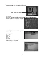
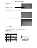
Page 37: ... of remote controller until appears the service menu 4 Set data of No 888 from 0 to 1 then press OK button RS232C cable should be connected 5 RS232C cable should be connected between TV set and PC 6 Appeared programe menu after double crick Hyper Termi nal I con Condition of Transfer Bit rate 115200 Data bit 8 Parity none Stop bit 1 Flow none 7 Crick Transfer then select File send 8 Select require...

Page 38: ...MODE YELLOW and Blue button of remote controller until appears the service menu 16 data of no 888 should be change back from 1 to 0 then press OK button 17 Turn Off the TV set 10 Click Send in the File send menu SERIAL RS 232C Connector pin specification pin signal name note 1 NC 2 RXD0 Data from PC 3 TXD0 Data to PC 4 NC 5 GND Set GND PC GND 6 NC 7 NC 8 NC 9 NC After confirmation of a soft versio...

Page 39: ...f BURN IN ON To escape from this mode press the SUB POWER button INPUT SELECT button and button at the same time and hold for more than 5 seconds Burn in mode will be released How to recover the remote and R side control key function If remote and R side control key cannot operate after miss set special function by front keys these functions can recover by below method Press the SUB POWER button I...

Page 40: ...L002 IC001 D601 D604 RL001 PC601 PC003 IC202 etc Q003 Q004 R004 R005 etc D001 STB NG NG NG open connector CN64 PDP module Va NG NG Q101 IC101 R004 R005 etc NG impedance check FUSE R004 R005 impedance check D001 impedance check Q003 Q004 impedance check Vs LINE impedance check Q101 Q201 IC220 Q200 D210 etc NG impedance check Q201 Q301 IC303 D310 etc PC201 PC202 D210 etc NG impedance check Q301 chec...

Page 41: ...tages applied to CN63 1 pin and CNPPS 3 8 pins of Power supply unit Power cannot be turned on LED does not light CN63 1 5V CNPPS 3 24V 8 10V Check Sub power FC PCB Power supply unit Main switch SW PCB AC Fuse F902 T6 3AH 250V Filter PCB AC inlet Re adjustment is reqired Plese refer to Power Unit Vs Va Adjustment page ...

Page 42: ...o input 10V PSP1 7 and 8 9 9 11 6 Power supply unit input 24V PSP1 3 and 4 23 75 26 25 Power supply unit input STB5 8V PSP4 1 and 2 5 5 6 1 Power supply unit Table2 Table of output by EPGgo signal input output signal name 42PD9700U C pin No value V From To output 5 5V PJB1 1 and 2 5 4 5 9 Bridge madia unit output 30V PJM1 1 31 3 33 6 Main CB output 10V PJM1 3 9 9 11 1 Main CB output 6V PJM1 5 5 4 ...

Page 43: ...es Are waveforms at pin 45 47 of PFM1 L R Check FC PCB Are waveforms at Are waveforms at pin 1 3 of PMD2 L R DTT pin 43 45 of I201 L R Check around Check DTT Module U101 and P702 on FC PCB PMF1 Are waveforms at pin 31 30 of IN01 L R Check around I201 Is waveform at pin 2 of XN01 Check around IN01 Is waveform at pin 14 of U101 Check around XN01 Check U101 Yes Check around I201 ...

Page 44: ... 43 45 of I201 L R Check around PMF1 No Yes Are waveforms at pin 59 61 of I201 L R Check I201 Yes No Are waveforms at pin 13 3 of I203 L R Check around I201 Are waveforms at pin 14 5 of I203 L R Check I203 No Yes Yes Check around I203 Are waveforms at pin 13 3 of IC808 Are waveforms at pin 7 8 of IC801 Check around IC800 Check IC801 Are waveforms at pin 1 2 3 16 of IC801 Are waveforms at pin 84 85...

Page 45: ...t pin 45 47 of PFM1 L R Check FC PCB Are waveforms at pin 45 47 of PMF1 L R Check around PFM1 Yes No Are waveforms at pin 43 45 of I201 L R Check around PMF1 No Yes Are waveforms at pin 59 61 of I201 L R Check I201 Yes No Are waveforms at pin 13 3 of I203 L R Check around I201 Are waveforms at pin 15 2 of I203 L R Check I203 Yes Yes Check Bridge Media Unit No ...

Page 46: ... of I404 Check around I401 Are waveforms at pin 24 25 26 27 31 63 of I404 Check I404 Is waveform at pin 30 of I405 Check around I404 Check around SPEAKER UNIT Check around PAS1 PAS2 Yes Yes No No No Are waveforms at pin 1 9 12 13 14 38 of I405 Yes Are waveforms at pin 4 8 10 of I406 Are waveforms at pin 1 5 13 of I406 Check I406 Check I405 Check around I405 Check around I406 Are waveforms at pin 1...

Page 47: ... around IC803 Check around PAF1 Check around PFA1 Yes No No Are waveforms at pin 6 9 of IC804 Yes Are waveforms at pin 45 47 of PFM1 Check IC804 Check around IC804 Check around PFM1 PMF1 Are waveforms at pin 2 4 5 6 10 11 of PFA䋱 Are waveforms at pin 29 38 40 of I600 Is waveform at pin 15 of IC803 No Yes Is waveform at pin 2 of IC802 No Yes Yes Check around IC803 Is waveforms at pin 3 6 of IC802 C...

Page 48: ... No Composit Video Yes RF Check I201 No Check U101 Trouble of Sub picture No Yes Check I501 Yes SCART Comp Check I601 and Input terminal Yes Check around I601 Yes Yes Check Q207 Q217 Q219 Check I201 and Input terminal Check DTT Module U101 and P702 on FC PCB Yes Yes Are waveform at TP605 Y TP606 Cb and TP607 Cr Are waveform at 2pin R 4pin G 6pin B of PMD1 RGB Input DTT SCART or Component Input exc...

Page 49: ...at 53pin CV of I201 Is waveform at 63pin CV of I201 Check Q604 Q605 Q606 Check I601 Yes Check I504 Yes Check I201 Check U101 Yes Check Q206 and Q511 Yes Yes Check Q515 Q516 Q517 Yes No RF Composit Video S Video No No RF or Composit Video No Yes RF or Composit Video No S Video Check I504 Check Q512 Q513 No No No No Check I201 and Input terminal Check I201 and Input terminal RF Input Yes RF No Compo...

Page 50: ...at 31pin H and 32pin V of I601 Is waveform at 150pin Y of I501 Is waveform at 44pin Y of I201 Component Video for 480i 576i Is waveforms at 152pin Y of I501 Is waveform at 148pin CV of I501 Is waveform at 44pin CV of I201 Is waveform at 63pin CV of I201 No No Yes Component Video except 480i and 576i Check I601 Yes Check I501 Yes Check I501 No Component Video for 480i 576i RF Composit Video S Video...

Page 51: ...601 Is waveform at 1pin CV of I504 Is waveform at 53pin CV of I201 Is waveform at 63pin CV of I201 No No No Yes Check I601 and Input terminal Check I602 Yes Check I601 Yes Yes Yes Component Video No RF Composit Video S Video RF or Composit Video Yes RF or Composit Video No S Video No No No RF Input No Composit Video Yes RF No Trouble of Sub picture Yes Yes Check I504 Yes Check Q512 Check I201 and ...

Page 52: ...n B and 160pin G of I501 No Check FC PWB Are waveform at TP608 Y TP609 Cb and TP610 Cr Are waveforms at 42pin Y 44pin Cb and 46pin Cr of I601 Are waveforms at 78pin Y 80pin Cb and 2pin Cr of I601 Check I601 Yes Check I504 Yes Check Q604 Q605 Q606 Yes Check Q515 Q516 Q517 Yes No No Are waveforms at 21pin Y 22pin Cb and 23pin Cr of I504 No Are waveforms at 35pin R 34pin G and 33pin B of I504 No Yes ...

Page 53: ... Table 1 Yes Yes No No 1 No Signal mode Horizontal frequency kHz Dot clock frequency MHz Remarks Signal Name Resolution Vertical frequency Hz 1 VGA 640 X 480 59 94 31 47 25 18 EIA 861B 2 576i 720 1440 X 576 50 00 15 63 27 00 EIA 861B 3 480i 720 1440 X 480 59 94 15 73 27 00 EIA 861B 4 576p 720 X 576 50 00 31 25 27 00 EIA 861B 5 480p 720 X 480 59 94 31 47 27 00 EIA 861B 6 1080i 50 1920 X 1080 50 00 ...

Page 54: ...e SUB POWER button of the monitor or the remote control Procedure 1 Press the SUB POWER button and button on the bottom of the monitor at the same time and keep it for more than 5 seconds after the power turned on 2 It generates red blinking series of the power indicator light 3 Any operation would cancel the Self Diagnosis mode 4 The next table shows the PDP PCB in which failure most probably wou...

Page 55: ...tor ZC HDMI IC Signal circuit self diagnosis function This function is for the failure of the signal circuit for example the phenomenon as below Sometimes power turns off abnormally Sometimes picture disappears abnormally To enter to this Self Diagnosis mode follow the next steps Preparation 1 The Power Cord should be connected to AC line and the Main Power switch should be turned on 2 Turn the po...

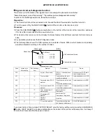
Page 56: ...01 MAIN V 44 PIN I501 YIN S VIDEO 44 PIN I501 CIN S VIDEO 43 PIN I501 YIN 3D 5 PIN I501 CIN 3D 7 PIN TP65 MY TP68 SY TP66 MPB TP69 SPB TP6A SPR TP67 MPR TP61 MH 5 0Vp p TP63 SH TP64 SV TP62 MV 1V 1H 0 3Vp p 1H 2Vp p 1H 1 0Vp p 1H 1 4Vp p 1H 1 2Vp p 1H 1H 1 2Vp p 1H 5 0Vp p 0 3Vp p ...

Page 57: ...62 PCB assembly MAIN 2 63 PCB assembly MAIN 3 64 PCB assembly MAIN 4 65 PCB assembly MAIN 5 66 PCB assembly LED PDP 67 PCB assembly SWIVEL 67 PCB assembly PCB assembly Filter Terminal 67 PCB PCB assembly PCB assembly PCB FC 71 PCB assembly FC 2 72 PCB assembly PCB assembly PCB assembly FC 5 75 PCB assembly FC 6 76 PCB assembly FC 7 77 PCB FC 78 PCB assembly FC 9 79 Basic circuit diagram list ...

Page 58: ...SM 011 POWER BOARD CIRCUIT SHEET 1 ...

Page 59: ...SM 011 POWER BOARD CIRCUIT SHEET 2 ...

Page 60: ...SM 011 POWER BOARD CIRCUIT SHEET 3 ...

Page 61: ...SM 011 POWER BOARD CIRCUIT SHEET 4 ...

Page 62: ...SM 011 POWER BOARD CIRCUIT SHEET 5 ...

Page 63: ...SM 011 MAIN BOARD CIRCUIT SHEET 1 ...

Page 64: ...SM 011 MAIN BOARD CIRCUIT SHEET 2 A WAKE UP MAIN 5 ...

Page 65: ...SM 011 MAIN BOARD CIRCUIT SHEET 3 ...

Page 66: ...SM 011 MAIN BOARD CIRCUIT SHEET 4 ...

Page 67: ...SM 011 MAIN BOARD CIRCUIT SHEET 5 MAIN 2 ...

Page 68: ...SM 011 MISC CIRCUITS TO MAIN PCB TERMINAL PCB POWER SWITCH PCB TO FILTER PCB SWIVEL PCB TO MAIN PCB FILTER PCB FROM AC INLET TO AC SWITCH PCB TO PSU LED PCB TO FC PCB NOT MOUNTED ...

Page 69: ...SM 011 SUB POWER BOARD CIRCUIT ...

Page 70: ...SM 011 CONTROL BOARD CIRCUIT ...

Page 71: ...SM 011 SOUND BOARD CIRCUIT ...

Page 72: ...SM 011 FC BOARD CIRCUIT SHEET 1 To IC905 Video BM Signal change CLAMP Switching To FC4 To coax change SW To FC4 To FC4 To FC4 Sub com ...

Page 73: ...SM 011 FC BOARD CIRCUIT SHEET 2 To I C103 Video RGB change FC com Sync processing To MAIN com cync detect To IC705 BM HDMI OTHER coax change PLL processing ...

Page 74: ...SM 011 FC BOARD CIRCUIT SHEET 3 ...

Page 75: ...SM 011 FC BOARD CIRCUIT SHEET 4 about 7mA It is 0 4V at 22V to in press it ...

Page 76: ...SM 011 FC BOARD CIRCUIT SHEET 5 Female BM VIDEO change To IC202ARGB AMP ...

Page 77: ...SM 011 FC BOARD CIRCUIT SHEET 6 To com To com Isometry GND guard Isometry GND guard Isometry GND guard Isometry GND guard Isometry GND guard Isometry GND guard ...

Page 78: ...SM 011 FC BOARD CIRCUIT SHEET 7 A B work C D work A B work C D work ...

Page 79: ...SM 011 FC BOARD CIRCUIT SHEET 8 ...

Page 80: ...SM 011 FC BOARD CIRCUIT SHEET 9 MAIN µ com ...

Page 81: ...SM 011 POWER BOARD ...

Page 82: ...SM 011 MAIN BOARD COMPONENT TOP SIDE ...

Page 83: ...SM 011 MAIN BOARD SOLDER BOTTOM SIDE ...

Page 84: ...OTTOM SIDE TERMINAL BOARD COMPONENT TOP SIDE SUB POWER BOARD COMPONENT TOP SIDE FILTER BOARD COMPONENT TOP SIDE SWIVEL BOARD COMPONENT TOP SIDE LED PDP BOARD LED LCD BOARD COMPONENT TOP SIDE COMPONENT TOP SIDE SOLDER BOTTOM SIDE ...

Page 85: ...SM 011 FC BOARD SOLDER BOTTOM SIDE COMPONENT TOP SIDE ...

Page 86: ...ub HDMI L R HP Amp BA3530FS L R Out L R In M CV SY M SC Video L R S CV S SY SC HP L R M OUT CV M OUT L R MCV SCV DET DET 6 75W P13B3253L SDA600x Teletext Decoder MAIN H V SUB H V H V OUT EPROM or FLASH SDRAM Main CV Y HD VD TEXT R G B TEXT Blank JIG for JTAG HMDI R G B 8bit HMDI H V HDMI DE HDMI CLK R G B 8bit OUT H V OUT DE OUT CLK OUT DDT R G B 8bit DDT H V DDT DE DDT CLK R G B CV L R R G B 8bit...

Page 87: ...50 65V Vs 75V 90V CPU IC202 Power Off 10V 24V Reg Ac in 5V AC Vsago Vcego STB3 3V Vcc5 1V EPGgo 24V 10V 3 3V STB5 8V R004 R005 RL002 RL001 D010 Aí D011 R020 R022 D001 D018 Q003 Q004 L005 370V Q501 Q520 Q301 Q201 Q220 Q101 T501 T301 T201 T101 IC261 IC160 D550 D551 D351 D260 D271 D251 D150 Relay Relay ...

Page 88: ... 5 GND 1 8V 1 8V 6 7 8 9 10 11 3 3V GND 1 8V PFJ2 ZH 12P PJF2 PH 12P 10V 1 STB5V DTT_POWER TV POWER 2 3 4 5 6 7 GND GND LEDOFF PFJ1 ZH 8P PJF1 PH 8P 10V 1 STB5V DTT_POWER TV POWER 2 3 4 5 6 7 GND GND LEDOFF 1 2 6V 6V 3 4 GND 3 3V GND 5 GND 1 8V 1 8V 6 7 8 9 10 11 3 3V GND 1 8V GND 12 12 GND SUB POWER EPGGO 8 EPGGO 8 VCC 1 P601 ZH 11P VCC GND 2 3 4 5 VCC GND GND 6 7 LCDGO 8 BL_ON CPUGO 9 10 11 IPWM...

Page 89: ...SET RS232C SW Audio SW1 Audio SW2 S RESET S FEW Sub L Sub R Sub Woofer S RXD GND GND Color_Sys FUNC_1 11 12 13 14 15 16 17 18 19 20 21 22 23 24 25 26 27 28 29 30 41 42 43 44 45 46 47 48 49 50 51 52 53 54 55 56 57 58 59 60 61 62 63 64 65 66 67 68 69 70 1 2 3 4 5 6 7 8 9 10 31 32 33 34 35 36 37 38 39 40 71 72 73 74 75 76 77 78 79 80 TV POWER BM MUTE RS232C TXD RS232C RXD S FCK S TXD GND GND A 9V 1 B...

Page 90: ...SM 011 WIRING ASSEMBLY DIAGRAM 1 ...

Page 91: ...SM 011 WIRING ASSEMBLY DIAGRAM 2 ...

Page 92: ...SM 011 WIRING ASSEMBLY DIAGRAM 3 ...

Page 93: ...SM 011 ASSEMBLY DIAGRAM ...

Page 94: ... before replacing PDP module Add holders before packing PDP module Joint Holder x8 Remove holders and attach handles for packing Attachment for packing Attach before packing panel module Panel A BUS R Logic PCB Panel A BUS L Y SUS PCB X SUS PCB ...

Page 95: ...THE UPDATED PARTS LIST FOR THIS MODEL IS AVAILABLE ON ESTA ...

Page 96: ...47 Milano Italia ITALY Tel 39 02 487861 Tel 39 02 38073415 Servizio Clienti Fax 39 02 48786381 2 Email customerservice italy hitachi eu com HITACHI Europe AB Box 77 S 164 94 Kista SWEDEN Tel 46 0 8 562 711 00 Fax 46 0 8 562 711 13 Email csgswe hitachi eu com HITACHI EUROPE S A S Lyon Office B P 45 69671 BRON CEDEX FRANCE Tel 33 04 72 14 29 70 Fax 33 04 72 14 29 99 Email france consommateur hitachi...

Reviews: