


9100A-017
7-15
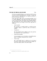
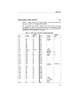
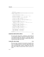
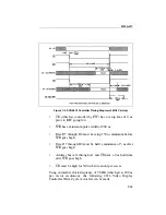
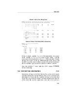
Figure 7-2. SCN2674 Controller Timing Diagram (4 MHz Version)
•
CE (which is controlled by PS7) has a setup time of 0 ns
prior to R/W going low.
•
WR has a minimum pulse width of 200 ns.
•
Data D7 through D0 must be setup 150 ns minimum before
WR goes high.
•
Data D7 through D0 must be held a minimum of 5 ns after
WR goes high.
•
Address bus A11 through A1 and CE have a 0 ns hold time
after WR goes high.
•
CE must be high for 300 ns between chip accesses.
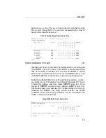
Using an internal clock frequency of 5 MHz (which gives 200 ns
per vector resolution), the following 2674 Video Display
Controller Write Cycle vector file can be made.
Summary of Contents for 9100A Series
Page 6: ...vi ...
Page 8: ...viii ...
Page 10: ...x ...
Page 14: ...9100A 017 1 4 ...
Page 24: ...9100A 017 3 6 ...
Page 44: ...9100A 017 5 4 ...
Page 58: ...9100A 017 6 14 ...
Page 83: ...A 1 Appendix A New TL 1 Commands ...
Page 84: ...9100A 017 A 2 ...
Page 87: ...clockfreq 3 For More Information The Overview Of TL 1 section of the Programmer s Manual ...
Page 88: ...clockfreq 4 ...
Page 91: ...drivepoll 3 For More Information The Overview Of TL 1 section of the Programmer s Manual ...
Page 92: ...drivepoll 4 ...
Page 104: ...vectordrive 4 ...
Page 107: ...vectorload 3 For More Information The Overview Of TL 1 section of the Programmer s Manual ...
Page 108: ...vectorload 4 ...
Page 116: ...9100A 017 C 2 ...
Page 117: ...9100A 017 C 3 ...
Page 118: ...9100A 017 C 4 ...


